Facebook
 Google
 GitHub
 Linkedin
Reevaluating the Toxicity of Semiconductor Manufacturing
The safety of semiconductor manufacturing employees is a top priority. Still, these facilities handle toxic materials that can pose a hazard to human health.
When it comes to producing critical electronics, it's crucial to consider costs beyond monetary investment. Worker safety is essential in manufacturing. Unfortunately, many microelectronics manufacturing processes involve toxic chemical elements that can pose health hazards.

Semiconductor manufacturing processes with corresponding toxic chemicals. Image used courtesy of EPA
What risks exist, and how are personnel working to mitigate them?
Understanding Potential Dangers
Semiconductor facilities utilize multiple liquids and solvents—acidic, alkaline, or otherwise—that can be as hard on human physiology as they are on the materials they treat.
Aside from being caustic, many commonly-used chemicals are known human carcinogens. Some examples that can carry high risk are toluene, acetone, methylene chloride, xylene, chloroform, and isopropyl alcohol. Others—like glycol ethers—may even cause reproductive harm.
Often, workers can accidentally absorb these substances through direct skin contact; however, direct contact isn't the only way to be affected. Inhalation of harmful gaseous byproducts like ozone, carbon monoxide, and phosgene can also cause numerous health issues, including skin irritation, eye damage, headaches, and digestion issues, among many others.
Fabricators establish safety procedures to minimize risks—in accordance with guidelines from OSHA, the CDC, ANSI, and SESHA. These safety standards often include personal protective equipment (PPE).
Material Hazards
Metals are undeniably crucial in semiconductor production. Cadmium, tellurium, gallium, mercury, and arsenic are cornerstone elements within specific chips. These elements are chiefly present within chemical compounds like mercury cadmium telluride or gallium arsenide. These compounds are favorable within semiconductors thanks to their electrical properties.

Semiconductor manufacturing employees wearing personal protection equipment. Image used courtesy of the Semiconductor Industry Association
However, each poses a fundamental hazard to human health during acute or repeated exposure.
- Arsenic exposure may cause swelling, skin irritation, anemia, leukocytopenia, and multiple forms of cancer (over extended periods). Acute ingestion can cause burning, stomach pain, nausea, vomiting, convulsions, coma, and even death.
- Mercury exposure is associated with nervous system issues, immune disorders, kidney damage, skin irritation, and eye irritation. The WHO considers it a top ten chemical of public health concern.
- Gallium is corrosive and harmful when inhaled—from a respiratory, nervous, and renal standpoint.
- Tellurium can cause eye, skin, and lung issues. Sustained inhalation can lead to pulmonary edema, liver and kidney damage, nervous system damage, and general fatigue or sickness.
- Repeat exposure to cadmium is attributed to cancer growth. It also impacts the cardiovascular, nervous, respiratory, renal, and gastrointestinal systems.
It is important to note that these metals can exist in different forms—whether they're solids, powders, or liquids. OSHA and other agencies define workplace exposure limits to these elements, while workers and floor engineers wear PPE to help restrict exposure.
Are Silicon Chips Hazardous After Manufacturing?
Even the small, metallic particles used during semiconductor production don't just disappear. These compounds can remain in finished semiconductor products, like solar panels. There's concern that these harmful nanoparticles may be released or leach into other materials during handling—thus contacting the skin or inadvertently entering the body.

Diagram showing the displacement of nanoparticles within the body and the possible effects. Image used courtesy of Chao Zeng
One way to help circumvent potential hazards is to move away from the toxic materials altogether.
Exploring Safer Alternatives
Since there are so many potential risks, there's a push to move away from periodic heavy metals toward organic compounds. Engineering researchers are proposing less toxic (or non-toxic) semiconductor materials, which function similarly to the currently-used materials. However, viability will depend on the application at hand.
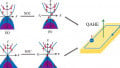
One promising semiconductor compound is Ca3SiO—comprised of calcium, silicon, and oxygen. Compounds like these are considered oxysilicides, which have previously been unable to emit infrared radiation. This limitation helped bring our existing toxic semiconductors into prominence. Thankfully, new research from Japan's National Institute for Materials Science and the Tokyo Institute of Technology has led to a breakthrough in direct transition semiconductor design.
These emerging chips may help power fiber-optic communications, night vision devices, and solar panels. The small bandgap characteristic of these chips will provide significant performance advantages moving forward. This characteristic is critical for absorbing, emitting, and detecting longer IR wavelengths. Another benefit is in thin-film applications, including those involving LEDs.
The Ecological Benefits of Non-toxic Semiconductor Materials
These compounds are far less toxic during manufacturing and thankfully pose minimum risks during handling—as one might experience during assembly or repair. There's also an added ecological benefit.
For every one person of the 7.8 billion people on Earth, each is producing 16 pounds of e-waste a year. Let's not forget commercial electronics and notably massive quantities of decommissioned solar panels. Instead of depositing vast amounts of heavy metals that could leach into groundwater or soils, we can discard eco-friendlier organic compounds.

E-waste statistics from 2019. Image used courtesy of Forti et al. and Global E-waste Monitor
These non-toxic alternatives won't be commercially viable for some time. Toxic compounds are still in use because of their exceptional conductive properties, which may be challenging to top without copious research.