
 Facebook
 Google
 GitHub
 Linkedin
Research Shorts: 5 Studies Make Headway in Lasers, Antennas, and Beyond
From tunable metamaterials inspired by chameleons to radiation-resistant organic solar cells, these discoveries address critical challenges in fields like defense, space exploration, communication, and manufacturing.
In this research round-up, we explore how innovations in materials science and engineering are pushing the boundaries of various fields. These innovations extend from chameleon-inspired tunable microwave absorbers to flexible organic solar cells for space.
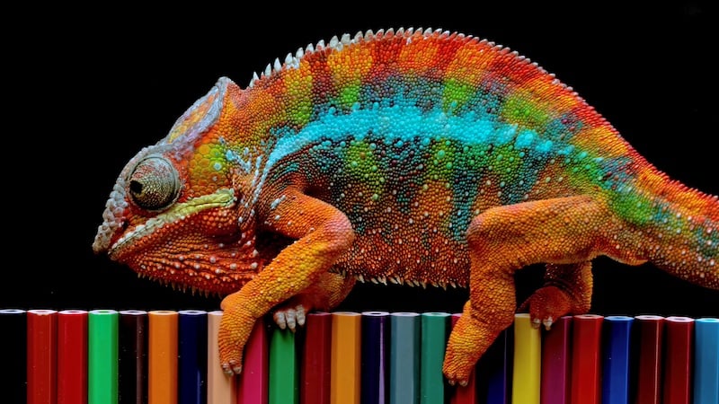
UC Berkeley has devised a new electromagnetic material inspired by color-shifting chameleons. Image (modified) used courtesy of Adobe Stock (under license)
1. Chameleon-Inspired Metamaterial Microwave Absorber
A research team led by UC Berkeley has developed a tunable electromagnetic material inspired by the chameleon's ability to adjust its color by altering photonic crystal spacing. This metamaterial microwave absorber features a crisscross truss structure that can mechanically expand or collapse to switch its electromagnetic properties.
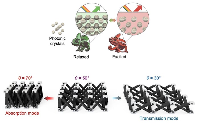
A chameleon’s color-changing mechanism (above) and the bioinspired tunable metamaterial microwave absorber (below). Image used courtesy of UC Berkeley
Machine learning and genetic algorithms optimized the design for specific responses, and 3D printing fabricated the structure. When collapsed, the material absorbs over 90% of microwaves in the 4–18 GHz range, effectively making it radar-invisible. In its expanded form, it allows up to 24.2% signal transmission, supporting communication. This dual functionality addresses longstanding challenges of fixed electromagnetic materials, enabling adaptability in dynamic environments.
The material has promising applications across defense, wireless communication, energy, and smart infrastructure. It could enable radar-invisible vehicles that still allow communication signals or smart windows that toggle between signal blocking and transmission for privacy and security. It may also improve the efficiency of systems harvesting electromagnetic energy for sensors and batteries.
2. CMOS-Compatible GaAs Nano-Ridge Lasers
Imec achieved a major milestone in silicon photonics by fabricating electrically pumped GaAs-based nano-ridge lasers on standard 300-mm silicon wafers. This development tackles the long-standing challenge of integrating scalable, CMOS-compatible light sources. Traditional approaches, like hybrid or heterogeneous integration, involve costly and resource-intensive processes with high material wastage.
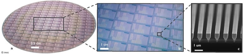
A 300-mm silicon wafer containing thousands of GaAs devices with a close-up of multiple dies and an SEM of a GaAs nano-ridge array after epitaxy. Image used courtesy of Imec
Imec’s solution leverages direct epitaxial growth of III-V materials on silicon using selective-area growth (SAG) and aspect-ratio trapping (ART). These methods significantly reduce crystal defects by trapping misfit dislocations in trenches. Additionally, nano-ridge engineering enabled the growth of low-defect nano-ridges with precise material control, achieving threading dislocation densities below 10⁵ cm⁻². The lasers incorporate InGaAs quantum wells in a p-i-n diode structure, capped with InGaP, and were produced entirely in a CMOS pilot line.
This innovation delivered room-temperature, continuous-wave lasing with a low threshold current of 5 mA and slope efficiency of 0.5 W/A, reaching optical powers of 1.75 mW at 1020 nm. These results set a new benchmark for wafer-scale integration of III-V materials with silicon, providing a cost-effective pathway for high-performance optical devices. Applications span data communications, machine learning, and AI, highlighting monolithic III-V integration's scalability and economic potential. Imec continues to refine its processes, focusing on near-term hybrid techniques, mid-term bonding technologies, and long-term direct epitaxial solutions to push this technology toward broader industry adoption.
3. Flexible, Radiation-Resistant Organic Solar Cells
University of Michigan researchers have presented a study demonstrating organic solar cells as an alternative to conventional silicon and gallium arsenide solar panels for space applications. Traditional materials are heavy, inflexible, and susceptible to proton radiation in space, leading to performance degradation. In contrast, organic solar cells, made from carbon-based materials, are lighter, flexible, and potentially more radiation-resistant.
The Michigan study tested these cells under simulated space conditions, specifically proton radiation, to evaluate their performance and identify causes of degradation at the molecular level. Organic cells made from small molecules showed no degradation after three years of radiation, while polymer-based cells lost half their efficiency due to side-chain cleavage, which created electron traps that hindered electricity flow. Researchers found that thermal annealing at 100°C could heal this damage by rebonding hydrogen atoms, restoring performance.
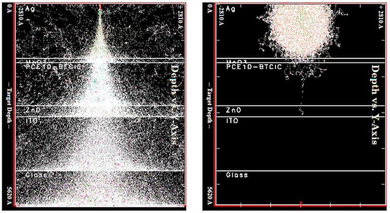
A simulation shows how deeply protons with higher energies of 100 kiloelectron-volt (keV) penetrate the solar cell (left) while another (right) shows how deeply protons with energies that typify the high end of the solar wind, 10 kiloelectron-volts (keV), penetrate the solar cell. Most don’t make it into the organic layer. Image used courtesy of the University of Michigan
The findings demonstrate the potential of organic solar cells to replace traditional materials in space missions. The study's simulations provided insights into proton penetration depths and molecular-level damage, contributing to the design of radiation-resistant materials. Challenges remain, such as ensuring the long-term reliability of thermal annealing and developing materials that inherently resist electron trap formation.
Further research aims to explore self-healing mechanisms in space conditions and alternative methods to address damage. With technology licensed by Universal Display Corporation and plans for further development at Nanjing University, these advancements could lead to lighter, more cost-effective, and robust energy solutions for future space missions.
4. A New CPD Manufacturing Technique for Lightweight Antennas
University of California researchers have introduced a new charge-programmed deposition (CPD) additive manufacturing technique for building lightweight antennas with complex geometries. Traditional manufacturing methods, like lithography and machining, cannot integrate materials and achieve intricate designs for modern applications such as 5G/6G, IoT, and satellites.
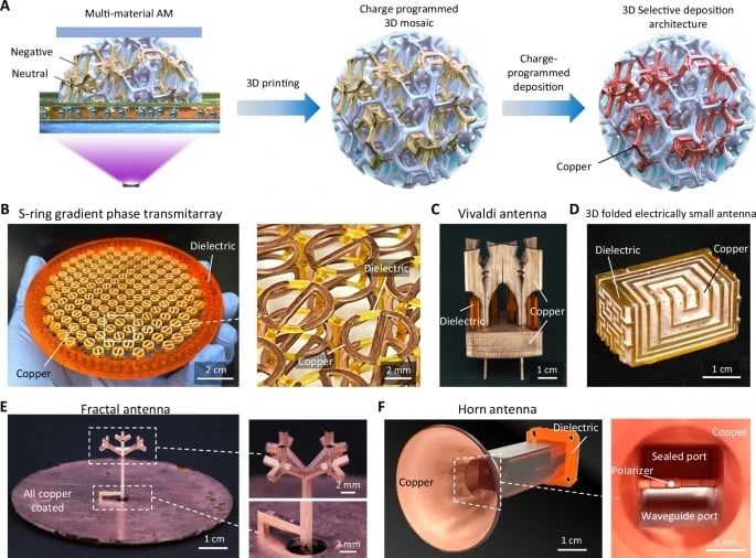
The image depicts (A) charge programmed printing and deposition scheme; (B) a gradient phase transmitarray with three layers of interpenetrating S-rings and dielectric materials; (C) a Vivaldi antenna; (D) a 3D-folded electrically small antenna; (E) a tree fractal antenna; (F) a horn antenna with a septum polarizer. Image used courtesy of the Nature
Current additive manufacturing methods fall short due to single-material constraints, complex processes, and post-sintering issues that degrade conductivity. CPD overcomes these limitations using a multi-material 3D printing approach to pattern surface charges for selective deposition of dielectrics and metals. The process eliminates the need for toolpaths or substrates and achieves fine feature resolution (18 μm) with high copper conductivity (4.9 × 10⁷ S/m). It enables significant weight reductions, including a 94% reduction in a transmit array antenna’s mass, while maintaining performance on par with traditional designs.
Key applications include lightweight antennas for aerospace, IoT, wearable electronics, and CubeSats, where weight is critical. The modular design enables scalable antenna production, demonstrated with 12-cm and 20-cm transmit arrays using stackable components. Tests of these transmit arrays and other CPD-fabricated antennas, such as horn antennas and gradient-phase transmit arrays, confirmed performance accuracy, low directivity variations, and excellent polarization purity.
Future work focuses on further automating the process, optimizing materials, and exploring multi-functional coatings like magnetic and piezoelectric materials to broaden industrial and research applications. This method offers a cost-effective and versatile solution for advancing antenna technology in weight-sensitive and high-performance applications.
5. UVC Micro-LEDs for Precision Photolithography
HKUST Engineering researchers have recently presented high-power AlGaN deep-ultraviolet (UVC) micro-LEDs for maskless photolithography. Their research highlights key challenges, such as the trade-off between resolution and light output power in miniaturized LEDs and the non-uniform emission in large arrays.
_images_.jpg)
The electroluminescence (EL) images demonstrate that devices of various sizes perform effectively at operational current densities, even for the smallest 3-μm device. The UVC micro-display can offer exceptional uniformity and significant light output power, enabling the successful implementation of the pattern transfer process. Image used courtesy of HKUST Engineering
Using advanced fabrication techniques, the team developed devices ranging from 3 μm to 100 μm, achieving a peak external quantum efficiency of 5.7% and a maximum brightness of 396 W/cm² for the smallest 3-μm LEDs. The researchers created a 320 × 140 UVC micro-display featuring enhanced heat dissipation and light extraction efficiency. They used this display to demonstrate maskless photolithography with precise patterning on photoresist films. Integrated reflective layers and optimized current spreading addressed previous limitations, achieving uniformity and high-resolution pattern transfers.
The HKUST team’s work overcame technical obstacles like wafer bowing, non-radiative recombination, and insufficient optical power. The team suggests they must further refine the epitaxial layer quality and light extraction techniques to scale the resolution to 2K–8K levels.
Applications extend beyond photolithography to semiconductor manufacturing, sterilization, and display technologies, potentially replacing traditional mercury-based lamps with more sustainable UVC sources. Challenges like high forward voltage and heat management in smaller devices remain areas for improvement to push commercial viability and performance.










Thank you for providing the exciting news items on one convenient page!
Very Cool!