Facebook
 Google
 GitHub
 Linkedin
Rounding Up Schottky Barrier Diode’s Exploits With Wide Bandgap Materials
Wide bandgap materials like SiC and GaN keep finding their way into more and more devices, like Schottky barrier diodes (SBDs). Let's take a look at some recent releases and check the status of GaN SBDs.
As the applications of semiconductor devices grow wider, manufacturing a power-efficient product is a primary concern for researchers and manufacturers.
One key component that has piqued the interest of researchers and manufacturers to meet the objectives in high-power and high-temperature applications is the Schottky barrier diode (SBD).
Due to the superior intrinsic material properties over silicon (Si), wide bandgap materials such as silicon carbide (SiC) and gallium nitride (GaN) are employed in the industry to meet the demands of low power consumption in power device applications. This need has led to the fabrication of SiC- and GaN-based SBDs.

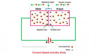
A general example of a Schottky barrier diode. Image used courtesy of Toshiba
The wide bandgap materials have proved to be a beneficial choice for high power and high voltage devices.
For instance, manufacturers utilize GaN in laser diode for optoelectronics applications. Also, in the past, designers used the material to fabricate high electron mobility transistors.
With that in mind, this article will look into some recent SBD's to hit the market, how the different semiconductor materials come into play and the continuing research into GaN SBDs.
Recent Schottky Barrier Diodes in the Market
Nowadays, data centers and communication devices demand efficient power supply to keep power equipment running. The semiconductors in these equipment exhibit steady-state loss when operated.
Fuji Electric's SDB for Data Centers and Base Stations
To solve this problem, Fuji Electric recently announced its 2nd-generation discrete silicon carbide-based SBD suitable for use in power supply equipment of data centers and communication base stations.
A thin substrate element distinguishes the family of the SDBs, which reduces the distance of current flow, thereby reducing the power loss in high-power equipment. It is said that the product is aimed at saving energy and attaining a decarbonized society.
ROHM's Side-steps Thermal Runaway
ROHM, a key player in the semiconductor industry, has also added 12 new products to its RBQ and RBR series of Schottky barrier diodes.

ROHM's latest SBDs. Image used courtesy of ROHM
A lower forward voltage is required for efficiency, however, this leads to a higher reverse current which may lead to the breakdown of a diode—a phenomenon known as thermal runaway.
ROHM’s series features a low forward voltage characteristic while maintaining a low reverse current to avoid thermal runaway and achieve improved efficiency.
The series aims to provide rectification of AC to DC, which makes it find applications in consumer electronics.
Si vs. SiC vs. GaN in SBDs
Though silicon possesses material properties suitable for protection and rectification in power device applications, Si-based diodes are already reaching their theoretical limits.
These limitations make it difficult to meet the demands of robust and efficient performance required in high power applications such as high blocking voltage, low switching loss, and high switching speed.
On the other hand, wide bandgap materials such as SiC provide a faster switching capacity and reduce power losses.
Researchers in manufacturing Schottky barrier diodes also hoping to exploit GaN. GaN-based Schottky barrier diodes could be operated at higher frequencies while maintaining a low power loss in power converters.
Researchers have noted that a high concentration and high mobility distinguish the 2D electron gas (2DEG) found in the GaN heterostructure. Due to this, researchers are motivated to exploit GaN in high-power applications in power electronic devices.
Research on Gallium Nitride-based Schottky Barrier Diodes
There have been several research experiments geared towards exploiting GaN for use in SBDs. These experiments are generally aimed at improving material quality and performance.
One such experiment, done at the Key Laboratory of Advanced Photonic and Electronic Materials at Nanjing University, China, yielded a novel discovery about GaN SBDs.
The researchers fabricated a GaN-based SBD with a breakdown voltage of 10.6 KV and a power figure of merit (or PFoM) of more than 3.8 GW/cm2. With this attained result, researchers discovered that GaN-based SBDs could be suitable for use in ultra-high voltage applications.

Structure of a GaN-based vertical power Schottky barrier diode. Image used courtesy of Sun et al
Furthermore, edge termination techniques have been recently employed by researchers to improve the intrinsic material properties of GaN-based vertical power SBDs.
Edge termination techniques include field plate, which is employed to reduce electric field crowding under reverse bias. The method is used to redistribute the electric field at the edge of the Schottky contact metal under reverse bias.
All in all, the advancements and benefits of SBDs are relatively clear and will continue to build up momentum as it investigates new semiconductor materials like GaN. It will be exciting to see when and if GaN-based SBDs will break into the market.
Interested in learning more about recent Schottky barrier diode advances? Read on in the articles down below.
ROHM’s Hybrid IGBTs Target Performance by Adding a SiC Schottky Barrier Diode
Silicon vs. Silicon Carbide: Schottky Barrier Diode Edition
Nexperia’s Trench Schottky Diodes Seize Power Efficiency