Facebook
 Google
 GitHub
 Linkedin
Samsung’s 8th-gen Vertical NAND (V-NAND) Enters Mass Production
The new generation of V-NAND marks a major memory milestone for the industry, with Samsung claiming highest bit-density.
The memory field is one of the most important subsets of the semiconductor industry, but also faces some of the most daunting challenges. A leader in this field is Samsung, which has been pioneering memory technologies, such as its vertical-NAND (V-NAND) flash memory, for almost a full decade.
Promising continued innovation, the company unveiled its future roadmap for memory technology last month, which included the announcement of its 8th and ninth-generation technology. This week, Samsung is making good on this roadmap as it announced that their 8th-generation V-NAND has entered mass production, marking a major milestone in their memory portfolio.

Samsung’s 8th generation V-NAND. Image used courtesy of Samsung
In this article, we’ll take a look at the history of Samsung’s V-NAND as well as the news surrounding its 8th-generation technology.
V-NAND’s History
As digital electronics grew to prominence throughout the past decades, NAND flash memory has become one of the most universal forms of non-volatile memory. Historically, the NAND flash architecture consisted of a 2D topology in which NAND cells were side by side and planar.
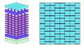
However, as the demand for bit density continued to increase, it quickly became apparent that this planar architecture would limit the ability to scale. To answer this challenge, the industry came up with 3D NAND, in which NAND cells were no longer planar, but stacked vertically on top of one another and connected in a layer-by-layer fashion. Samsung was the first company to commercialize this technology with the introduction of its first-generation V-NAND technology in 2013.

3D NAND architecture. Image used courtesy of Enterprise Storage Forum
This original generation of V-NAND only consisted of 24 layers, which, compared to their 2030 goal of 1000 layers, is seemingly trivial. Yet, as the company innovated with new generations of their V-NAND, they began to encounter issues with adding more layers in the form of physical limitations related to the height of the device. Samsung then addressed this problem by scaling down the surface area and height of each individual cell.
By doing this, Samsung managed to reduce their individual cell volumes by up to 35%, enabling more layers to be added without increasing the height of the solution. A prime example of this is their 176-layer 7th generation NAND which is the same height as their 6th generation solution despite having an extra 40 layers.
8th Generation V-NAND
Now, Samsung is continuing to add to the rich history of its V-NAND product line with the recent announcement of its 8th-generation V-NAND reaching mass production.
The new V-NAND solution is a 1-terabit triple-level cell (TLC) offering that, according to Samsung, features the industry’s highest bit density. Samsung attributes this achievement to its ability to enhance the “bit productivity” per wafer. By this, Samsung means that they increased their I/O speed by 1.2X to 2.4 Gbps.
With these improvements, Samsung expects their 8th generation V-NAND to find critical applications in memory-intensive environments such as enterprise servers.
Adding to V-NAND History
As the demand for bit density increases, Samsung has continually met the call with innovations to their V-NAND solution. Fortunately, they have not let up on this trend, although many are skeptical of their goals of extending their V-NAND to 1,000+ layers in the next decade. No doubt it will be a difficult pursuit, but, if history is any indicator, Samsung will find a way to make it possible.