Facebook
 Google
 GitHub
 Linkedin
ST Hits an “Industry First” With 0.5 Mpixel iToF 3D Image Sensor
Targeting a breakthrough in digital vision, the ST’s family of high-resolution indirect Time-of-Flight (iToF) sensors aims to improve efficient depth imaging in devices that perform 3D imaging functionalities.
Capturing 3D images has been one of the growing demands of applications in cutting-edge technological devices that perform computer vision operations. Thus, computer vision engineers provide 3D imaging solutions based on Time-of-Flight (ToF) technology in smartphones and other camera-system devices.
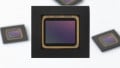
STMicroelectronics, hoping to capitalize on the boom for 3D sensing, has developed an iToF back-side illuminated (BSI) depth image sensor.

ST’s new product is fabricated on 40 nm stacked wafer technology. Image used courtesy of STMicroelectronics
Before diving into the new sensor, it's important to address what an iToF sensor is, how it compares to regular ToF sensors, and how it attempts to improve the performance in 3D imaging sensing?
First, let’s take a look at ToF technology. Then, dive deep into the new 3D imaging solution from ST.
Direct Vs. Indirect Time-of-Flight Sensing
Simply put, ToF technology is about measuring the time for a wave (such as a light wave) to travel from a ToF sensor (source) to a target or object (destination) and back.
The ToF technology utilizes the light from a ToF sensor to scan the surrounding for the object. The light emitted from a ToF sensor could hit an object and get reflected back at a distance ranging from 2 m to 10 m.
In general, ToF sensors are simple to design and use compared to other 3D imaging techniques such as stereo vision. On top of this, the sensors have a great processing speed and are compatible with smaller processors.
However, one drawback is that the accuracy of a ToF sensor could reduce in surroundings that reflect light in different directions and in objects that create multiple reflections when hit with light. The ToF technology also has less accuracy compared to 3D profiling.
All in all, ToF technology could be majorly classified into two types: direct and indirect.

Phase-shift is measured to give the distance between the sensor and the object in an indirect Time-of-Flight sensor. Image used courtesy of Terabee
While a dToF sensor only sends out light pulses to the target object and calculates the time it takes to be reflected back, an iToF sensor emits out a continuous and modulated light wave to the target object, and the phase shift of the reflected light is measured to calculate the distance between the sensor and the object.
Generally, ToF sensors find applications in a wide range of areas including autonomous robots for assembling line automation, motion detection and recognition, and in smartphones.
Introducing the Novel ST’s 3D iToF Sensor
Now that a general understanding of ToF is better understood, let's take a look at ST's latest sensor, the VD55H1, which claims to be the industry's first 0.5-megapixel 3D depth image ever manufactured.
Thanks to a 672 x 804 BSI pixel array for iToF depth sensing, VD55H1 leverages the iToF technology to map 3D surfaces and accurately measures distance up to half a million points.

The VD55H1 block diagram. Image used courtesy of STMicroelectronics
As a typical iToF sensor, objects could be detected up to 5 m from the light source when the product emits light. In addition, this distance is known by measuring the phase shift between the reflected signal and the emitted light wave.
The product leverages 40 nm stacked wafer technology for the fabrication process, boasting a small size of 4.5 mm x 4.9 mm.
Due to its multi-frequency operation, advanced depth-unwrapping algorithm, low pixel noise floor, and high pixel dynamic range, ST claims that the 0.5-megapixel 3D depth image sensor boasts high measurement accuracy.
Furthermore, the product finds applications in smartphones, AR/VR applications, and robotics.
All in all, the iToF 3D depth image sensor aims to meet the growing demands of efficient 3D depth imaging in a wide range of applications and to help round out ST's FlightSense ToF sensor portfolio.