Facebook
 Google
 GitHub
 Linkedin
Three’s a Crowd—YTMC Throws Its Own 3D NAND Into the Ring
Summer 2022 is turning out to be a hot one for the memory industry, with not just one, not just two, but three announcements from chipmakers relating to advanced 3D NAND production.
The boom of NAND developments continues with China’s Yangtze Memory Technologies Co Ltd (YMTC) announcing its 232-layered X3-9070 3D NAND chip at the 2022 Flash Memory Summit. This announcement follows that of US’ Micron and South Korea’s SK hynix, boasting their own latest-and-greatest 3D NAND developments.

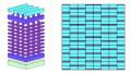
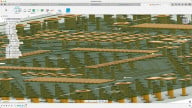
YMTC’s latest X3-9070 3D NAND chip. Image used courtesy of YMTC
The X3-9070 NAND chip is reported to have the following specs:
- An I/O speed of up to 2400 MT/s (ONFI 5.0 compliant)
- A 1 TB storage capacity in a mono-die footprint
- A 6-plane architecture that can support simultaneous independent operations to improve sequential and random access I/O operations
- A 50% boost in performance and a 25% decrease in power consumption compared to previous generations
Specifics power consumption and die volume were not made available. The X3-9070 chip is the fourth generation of 3D NAND from YMTC and uses the third generation of Xtacking architecture.
While the announcement introduces an intriguing new option, it is not clear when YMTC will be able to make the leap to mass production to catch up to competitors and compete for a larger market share. Although earlier in the year, Apple was reportedly seeking to diversify its supply chain and was testing out YMTC's flash memory.
With this announcement in mind, let's look at TMTC's Xtacking architecture and how its NAND innovation compares to others.
YMTC and Xtacking Architecture
According to YMTC's website, the company is headquartered in Wuhan, China, and began 3D NAND R&D in 2014. The company boasts of manufacturing the first Chinese 3D NAND memory in 2017.
Subsequent iterations have resulted in what the company calls the Xtacking architecture. Like other chipmakers, YMTC's strategy to improve the performance and memory density of 3D NAND involves minimizing the die size and building upwards to increase transistor density per mm2.
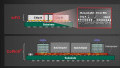
Xtacking appears to achieve this by fabricating the memory cell array wafer and periphery wafer in independent processes before fusing them together using "billions" of vertical interconnect accesses (VIAs) that form the electrical connection between the two.

Xtacking consists of fabricating periphery and memory array wafers independently. Screenshot used courtesy of YMTC [video]

Xtacking then fuses the periphery and memory array wafers together. Screenshot used courtesy of YMTC [video]
How Does YMTC Stack Against the Competition?
Both Micron and Sk hynix are taking the CMOS-under-array strategy (although Sk hynix specifically calls this 4D NAND), where the peripheral layer forms the bottom of the stack, with the memory cell arrays on top. This strategy differs from the conventional architecture, where the peripheral circuitry is laid horizontal to the memory cell arrays.

CMOS-under-Array architectures place the peripheral circuitry beneath the memory cell arrays. Image used courtesy of Micron
In Micron's latest announcement, its chip will also be 232 layers and will go into production at the end of the year. This chip will also feature I/O speeds of up to 2400 MT/s (ONFI 5.0 compliant), a 6-plane architecture, 1 TB storage capacity on an 11.5 mm x 13.5 footprint.
For Sk hynix, its announcement adds a few more layers for a total of 238 layers and is expected to go into production in the first half of 2023. The company has already shipped samples with 2.4 Gbps transfer speeds and a storage capacity of 512 GB per chip.

NAND flash manufacturer revenue by quarter in USD. Image used courtesy of Statista
Taking a step back and looking at how the various players in the NAND flash market performed, in Q1 of 2022, Samsung by far remains the lead in NAND revenue (6.32 billion), followed by Kioxia (~3.38 million), and not trailing far behind is Sk hynix (~3.22 billion). Micron's revenue was posted as ~1.95 billion. The "other" category where YMTC exists totals ~0.79 billion.
The competition remains fierce not only for YMTC but for Micron and Sk hynix as well.
US CHIPS For Making Chips
While all the excitement is happening in the flash memory market, the US just passed the aptly named CHIPS and Science Act that will see an investment of $52.7 billion to subsidize US-based semiconductor R&D and manufacturing.
Part of the momentum for the act came from a combination of the desire to be more independent from the global supply chain, which has struggled over the past several years to serve worldwide demand, and concerns over the security of the supply chain. This investment could also prevent things like the 2020 acquisition of US-based Intel's NAND memory business by Sk hynix from happening again in the near future.
The objectives of the CHIPS Act are not entirely unlike China's National Integrated Circuit Industry Investment Fund, which provides state funding to the Chinese semiconductor industry. YMTC receives investment from this fund to help the company compete.
The CHIPS Act may complicate things for YMTC and its latest announcement—if Apple is still seeking to diversify its supply chain, it may be possible that more US-based options will be available in the coming years.
A more competitive global market will hopefully mean more innovation, competitive pricing, and a more robust global supply chain in the future. Three back-to-back announcements of upcoming 3D NAND chips may be just the beginning.