 Facebook
 Google
 GitHub
 Linkedin
Wi-Fi Is a Power Guzzler. New Multi-Protocol Modules May Change the Game of Battery-Based IoT
Wi-Fi's high power consumption represents a serious challenge to battery-powered IoT products. But this may no longer be a problem with the digitally-dominant advanced radio architecture of two new modules from Innophase.
Although you can find IoT products based on wireless protocols such as Bluetooth, Zigbee, and Wi-Fi, none of these wireless technologies are originally designed for IoT applications.
For example, Bluetooth (IEEE 802.15.1) was originally developed to provide wireless connectivity between a computer and its peripherals. IEEE 802.15.4, which is used in Zigbee, was built as a low-power, low data rate alternative to Bluetooth. And the Wi-Fi standard (IEEE 802.11) was created to provide an Ethernet-based connection using wireless communications. That’s why Wi-Fi has a longer range and higher power consumption compared to Bluetooth and 802.15.4.
Bluetooth, Zigbee, Wi-Fi: What's the Best Option for Battery-Based IoT?
Among standards such as Bluetooth, Zigbee, and Wi-Fi, the Wi-Fi standard can be an appealing choice for many IoT applications because of its longer range, native IP connectivity, and high bandwidth. However, standard Wi-Fi protocols burn a lot of power, presenting a serious challenge to battery-powered IoT products.
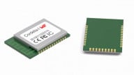
To address this problem, InnoPhase, which is a fabless semiconductor company specializing in low-power wireless solutions, has introduced the Talaria TWO modules, INP1010 and INP1011. According to Innophase, the Talaria TWO platform may introduce significant power savings for Wi-Fi-connected, battery-based IoT devices.
Innophase's director of product marketing Robert McCormick says it's possible that this solution may even replace low-power protocols like Zigbee and Z-Wave.
"Almost everybody has a Wi-Fi router in their house and business, but not many have a separate Zigbee router," he explains. "Our unit can match Zigbee power levels... so I think those low-power-specific protocols will go away and Wi-Fi will take over in their place."
What Is the PolaRFusion Architecture?
Integrated into the Talaria TWO modules is the Talaria TWO SoCs, which are said to add Wi-Fi connectivity to power-constrained IoT applications. It’s a highly-integrated, single-chip wireless solution based on a patented technology called PolaRFusion.
The inspiration for the PolaRFusion architecture came from Innphase's CEO, Dr. Yang Xu. Years ago, Xu's wife, a medical professional, was working with small swallowable pills that acted as cameras down the patient's digestive tract, sending information to doctors wirelessly. To work around the high battery consumption of these devices, Xu developed a new digitally-based architecture that consumed less power. He ended up with a polar radio architecture, which later matured into PolaRFusion technology.
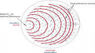
PolaRFusion is a digitally-dominant advanced radio architecture that uses the polar representation to encode/decode information. This architecture contrasts conventional radio architectures that have several power-hungry analog blocks in the frontend circuitry and are based on in-phase and quadrature (I/Q) paths (or the Cartesian representation).

Cartesian coordinates compared to polar coordinates. Image used courtesy of InnoPhase
According to InnoPhase, the PolaRFusion transceiver replaces many of the analog blocks of a conventional radio with digital circuitry. This reduces the system power consumption significantly and facilitates adding Wi-Fi connectivity to battery-powered IoT products.
McCormick notes that because PolaRFusion is digitally based, it "gives us the ability to do some programmability, which means that within the same radio, we can have both Wi-Fi and BLE."
Key Specifications of the Talaria TWO Modules
The Talaria TWO modules incorporate an embedded 80 MHz Cortex-M3 microcontroller to accommodate both system control and optional user applications. Besides, the single-chip wireless solution includes 512 KB SRAM and 2 MB Flash memory. This integrated approach is key to reducing the footprint and power consumption of the system.

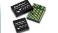
INP1010 and INP1011 block diagrams. Image used courtesy of Innophase
The SoC is a multi-protocol wireless platform that supports Wi-Fi 802.11 b/g/n and BLE 5.0 standards. It offers a very low power-save current consumption (DTIM10 with 75 µA). Such power save modes can reduce the power consumption of the Wi-Fi circuitry by a factor of eight in certain applications.
Another interesting feature of the Talaria TWO SoC is its advanced security elements including hardware-based crypto engines, encrypted flash, and support for unique ID per device.
As mentioned before, the company has employed innovative circuit techniques such as the advanced PolaRFusion radio architecture to reduce the system's power consumption. Two other techniques that contribute to the system's power advantages are a patented low-power digital power amplifier (DPA) and a high-performance low-noise amplifier (LNA) called flexLNA.
Reducing the Transmitter Power Consumption
InnoPhase attempts to reduce the power consumption of the transmitter by employing a more efficient power amplifier.
In general, power amplifiers are the most power-hungry building blocks of an RF transceiver. InnoPhase claims that it has invented an efficient digital power amplifier (DPA) for its Talaria TWO wireless platform.
While the company has not released many technical details about its DPA, DPAs in general encode the baseband information in a pulse train so the amplification can be achieved by means of a power switch. Just before the antenna, a bandpass filter is used to restore the analog signal from the pulse sequence. The basic idea is shown in the following figure.

Block diagram of a digital transmitter. Image used courtesy of Andreas Wentzel, Florian Hühn, Wolfgang Heinrich
Now, let’s take a closer look at the company’s patented polar receiver architecture.
A Digitally-Dominant Polar Receiver
The block diagram of InnoPhase’s patented polar receiver is shown in the following figure.

Block diagram of the Innophase polar receiver. Image extracted from InnoPhase polar receiver patent
The basic operation of this receiver can be summarized as follows:
- The received RF signal is amplified by a wide-band low-noise stage (block denoted by 104).
- The output is then applied to band-specific low-noise amplifiers (blocks 106, 108, 110) for further amplification. This stage performs some band-pass filtering. Note that several band-specific amplifier stages can be utilized in parallel to receive and decode signals in different frequency bands. For example, while one amplifier stage is incorporated for 800 MHz to 1.6 GHz, another amplification stage (in parallel) receives 1.6 GHz to 3.2 GHz.
- The output of the appropriate band-specific amplifier is injected into an injection-locked oscillator (block 122). The phase of the oscillator output is further processed through the frequency divider and TDC stages (blocks 124 and 126) to determine the phase of the input signal.
- A frequency multiplier along with a Gilbert cell (blocks 130 and 132) are used to extract an analog signal proportional to the amplitude of the received RF signal.
- Digital equivalents of the amplitude and phase information are obtained and the result is applied to a CORDIC circuit to extract the I/Q representation of the received signal.
Many building blocks of the above receiver can be implemented using digital circuitry. For example, the oscillator can be an injection-locked ring oscillator. Being mainly in the digital domain allows us to reduce the number of power-hungry analog blocks and take advantage of Moore’s law in our receiver architecture.
How Does a Polar Receiver Compare With N-Path Filtering?
A polar receiver such as the one briefly discussed above incorporates several interesting techniques to arrive at an efficient wireless solution; however, I was wondering how this technology can be compared with N-path filtering.
N-path filters are continuous-time switched-capacitor filters that can be used to implement high-Q bandpass and bandstop RF filters. This filtering technique was originally proposed and analyzed in the 1960s, but they were largely forgotten until about a decade ago when RF designers noticed that using the switches readily available in modern CMOS technologies, high-Q RF filtering based on the N-path technique is achievable.
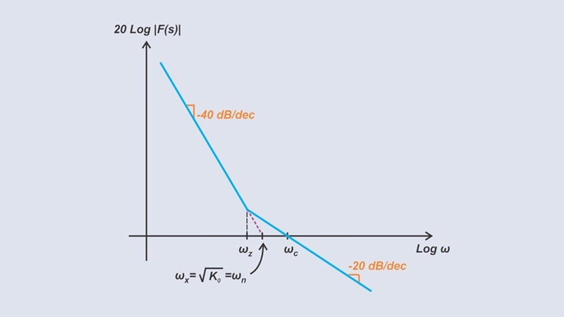
The following figure illustrates an LNA that uses N-path filtering.

The diagram on the left shows an initial attempt at front-end implementation while the graph on the right illustrates the frequency response to LNA output. Image used courtesy of Joung Won Park and Behzad Razavi
The transistors in the feedforward path are the amplifying stages of the LNA. These are the only transistors of the structure that are in the saturation region. The feedback path is denoted by “Bank 1,” which consists of eight parallel branches of switched capacitors. The figure shows only one of these branches. Note that the transistors in the feedback path act as switches and can take advantage of Moore’s law.
The above figure also depicts the frequency response of this LNA. Note that its 3-dB bandwidth is 300 kHz at around 1 GHz. Hence, it is possible to perform channel selection at RF. The I/Q representation of the received signal can be obtained directly from the voltages on the feedback capacitors (CF).
This circuit needs multi-phase clock generation for driving the switches. Moreover, the transistors used for the switches should be very large to achieve a small on-state resistance. This circuit seems to be much simpler than a polar-based architecture such as the one discussed above.
How do you think a polar receiver compares with the N-path LNA shown above? Share your ideas in the comments below.
Related Content


“based on a patented technology”... It’s Zigbee all over again. No thanks.