Facebook
 Google
 GitHub
 Linkedin
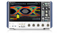
X-FAB Announces Substrate Coupling Analysis Tool To Combat Troublesome Parasitic Effects
A new tool from foundry group X-FAB aims to mitigate the negative effects of substrate coupling in IC design.
A new tool from foundry group X-FAB aims to mitigate the negative effects of substrate coupling in IC design.
SubstrateXtractor is a new tool from German analog/mixed-signal semiconductor foundry group X-FAB that enables engineers to uncover unwanted substrate couplings early in the design process. The tool hopes to solve the issue of identifying parasitic effects of substrate coupling in IC design, a problem that has persisted over the last quarter century.
What Is Substrate Coupling?
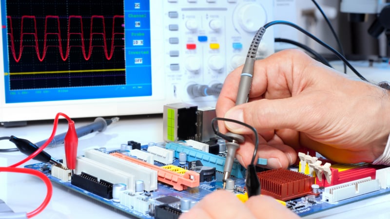
Substrate coupling is a defect wherein a signal may "couple" across a substrate from one node to another. Another way of putting it is that it is the "coupling of digital switching noise to analog/RF circuits through substrate." Other forms of coupling are possible—including coupling through power supplies, mutual inductance, and capacitive coupling—though substrate coupling is reportedly the most common.
Substrate coupling noise can cause several issues, including signal leakage and voltage fluctuations, and can affect chip-level performance. It is part of one of the most challenging parts of mixed-signal IC design, noise coupling.
This is most commonly seen in mixed-signal ICs, especially RFICs (radio frequency ICs) where both analog and baseband digital signal circuitry is present.
Designers are packing ever-more circuitry into less and less area, and signal speeds keep on increasing. So, it’s no wonder that unwanted substrate couplings can have a negative on impact IC development. These unanticipated, parasitic effects can wreak havoc on completion schedules for analog and high voltage designs—and can even crop up later, causing device failure.

Image from X-FAB
Even if issues noticed early in the design phase, engineers will nonetheless have to solve them by taking a slow and laborious ‘trial and error’ approach. The result is that schedules can slip by weeks while top designers will have no choice but to try out different design iterations, hoping to find a solution. It is this set of challenges that X-FAB hopes to target with this new tool.
X-FAB Addresses Large Signal Analysis
SubstrateXtractor from X-FAB is the semiconductor industry’s first commercially available tool dedicated to addressing the simulation of large signal substrate parasitic effects. What this means is that the tool enables analysis that takes into account many variables, such as gain and power supply levels changing simultaneously. It also means that the tool does not assume that components are operating in a near-linear manner about their prescribed operating points.
SubstrateXtractor works in conjunction with X-FAB’s established simulation libraries. It was created as a collaboration between X-FAB and Swiss EDA (electronic design automation) software vendor PN Solutions. SubstrateXtractor is based on PN Solutions' innovative PN Aware product, which is a substrate tool created in partnership with Cadence, the distinguished Swiss institute EPFL (École Polytechnique Fédérale de Lausanne), and Venture Kick, a Swiss accelerator program.

A screengrab of PN Aware. Image from PN Solutions
SubstrateXtractor's unique functionality is that it allows engineers to investigate where potential substrate coupling issues could occur and make the changes necessary to eliminate them (via better floorplanning, guard rings, etc.) before the initial tape-out has even begun.
Working with SubstrateXtractor
The goal is for engineers employing SubstrateXtractor to be able to look "under the hood" to gain full visibility of all the active and passive elements within a substrate. Within the software, engineers are able to experiment with different simulations in order to find a design concept that delivers maximum substrate coupling immunity within the project’s particular parametric constraints.
Costs will be reduced by determining the minimum number of substrate contacts and guard rings needed for a project. This will allow for more effective utilization of the available area.
As Joerg Doblaski, Director of Design Support at X-FAB puts it, “layout engineers will be able to uncover any adverse substrate effects early on in the development cycle and subsequently mitigate them.” He goes on to explain that “This will make IC implementation procedures far more streamlined and quicker to complete, avoiding the need to rework designs to increase levels of optimization, and resulting in significant cost savings.”
SubstrateXtractor will be integrated into X-FAB’s process design kit (PDK). It will first be available for use with X-FAB's XH018 high-voltage 0.18µm mixed-signal CMOS offering.

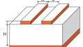
A cross section of the XT018 CMOS device. Image from the XT018 datasheet
A version for the XP018 power management process is expected to follow.
Around the Industry
In this case, it might be more correct to say "around the research labs" because the negative effects of substrate coupling are well known and there have been many academic papers written about the issue.
At this time, however, it appears that X-Fab and its partner PN Solutions may well be the only source with a commercial product available directly to engineers. If you're aware of other tools that serve a similar purpose, please tell us about them in the comments below.
You can read more about X-FAB's work on galvanic isolation semiconductor processes here.
Related Content