Facebook
 Google
 GitHub
 Linkedin
Build an Instrumentation Amplifier with Picoamp-Level Input Bias Current
Discover how the LT1079 quad op-amp minimizes sensor loading in battery-powered designs. Active cancellation and an onboard bridge network ensure maximum precision for resistive sensors.
The Instrumentation Amplifier with Bias Current Cancellation is a high-precision amplifier module built around the Analog Devices LT1079 micropower quad op amp. It is designed to measure very small signals from sensors while introducing almost no loading error on the source. The design uses three of the four op amps in the LT1079 in a classic three-amplifier instrumentation configuration, with the fourth section reserved for bias-current cancellation.
The module accepts a differential input through a 6-pin header and delivers a single-ended, ground-referenced output through a 4-pin header. Six 0805 SMD resistors — R1, R4, R5, R12, R13, and R16 — form a bridge network at the input, allowing the amplifier to interface directly with bridge-type sensors such as strain gauges and resistive bridges. A single 9 V DC supply powers the entire board, and an onboard LED indicates that power is present. The assembled board is shown in Figure 1.
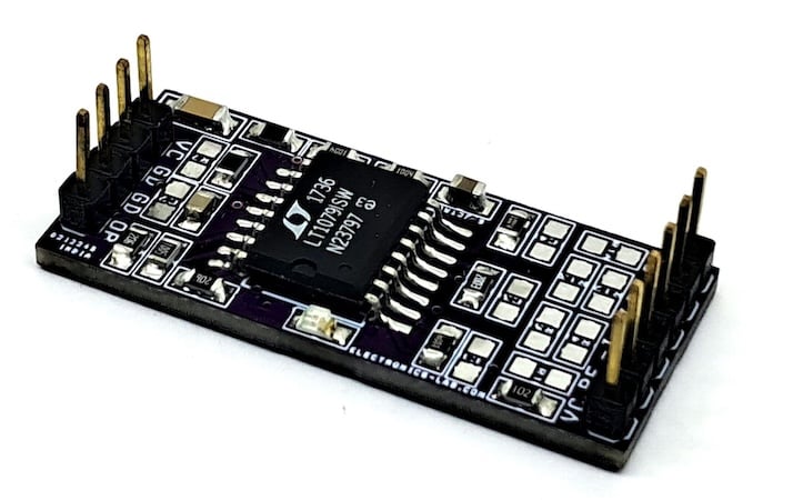
Figure 1. The assembled Instrumentation Amplifier with Bias Current Cancellation module.
The LT1079 draws very little supply current while still delivering low offset voltage and low noise. This makes the module well-suited to battery-powered instrumentation and sensor front-ends where both precision and low power draw matter.
Specs and Features
- Supply voltage: 9 V DC
- Output range: 4 mV to 8.2 V
- Key IC: LT1079 micropower quad op amp
- Gain: (1 + 2R3/RG) × R9/R2 = 100
- Input bias current: typically less than 150 pA
- Input resistance: 3R = 30 MΩ
- Gain bandwidth: 1.8 MHz
- Onboard power LED
- Header connectors for input, output, and power
- PCB dimensions: 36.99 mm x 16.19 mm
How It Works
The LT1079 is a micropower quad op amp in a standard 16-pin package. It is optimized for 5 V single-supply operation, though ±15 V operation is also specified. Most micropower op amps sacrifice precision, noise, speed, or output drive to save current. In contrast, the LT1079 cuts supply current without sacrificing performance.
The LT1079 achieves the lowest offset voltage of any dual or quad non-chopper-stabilized op amp. Its offset current, noise, slew rate, and gain bandwidth product are two to ten times better than earlier micropower models. Its voltage noise 1/f corner sits at 0.7 Hz—at least three times lower than any monolithic op amp. This provides low-frequency noise performance typically seen only in high-current devices.
The device can run from a single supply as low as one lithium cell or two Ni-Cad batteries. Its input range extends below ground. While sinking current, its all-NPN output stage swings within a few millivolts of ground, eliminating the need for power-consuming pull-down resistors.
On this board, three internal op amps form the instrumentation amplifier signal path. Two serve as input buffers, followed by a difference amplifier that sets an overall gain of 100. The fourth op amp combines with resistors R10, R17, and R18 to form a bias current cancellation loop, removing input bias current before it introduces sensor errors. Bridge resistors R1, R4, R5, R12, R13, and R16 allow the input stage to interface directly with resistive bridge sensors.
Schematic and Bill of Materials
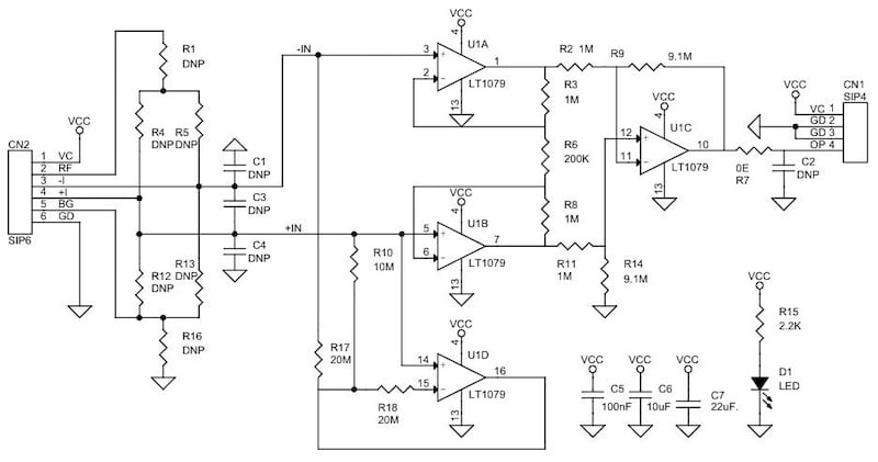
Figure 2. Schematic of the Instrumentation Amplifier with Bias Current Cancellation.
The bill of materials is shown in Table 1.
Table 1. BOM for Instrumentation Amplifier with Bias Current Cancellation.
| REF | DESCRIPTION | QTY | MFG | SUPPLIER | PART NO. |
| CN1 | 4-pin male header, 2.54 mm pitch | 1 | WURTH | DIGIKEY | 732-5317-ND |
| CN2 | 6-pin male header, 2.54 mm pitch | 1 | WURTH | DIGIKEY | 732-5319-ND |
| R1, C1, C2, C3, R4, C4, R5, R12, R13, R16 | DNP | 10 |
|
|
|
| C5 | 100 nF / 50 V ceramic SMD, 0805 | 1 | YAGEO/MURATA | DIGIKEY |
|
| C6 | 10 µF / 25 V ceramic SMD, 0805 | 1 | YAGEO/MURATA | DIGIKEY |
|
| C7 | 22 µF / 25 V ceramic SMD, 0805 | 1 | YAGEO/MURATA | DIGIKEY |
|
| D1 | LED, red, 0805 | 1 | OSRAM | DIGIKEY | 475-1278-1-ND |
| R2, R3, R8, R11 | 1 M, 1%, SMD, 0805 | 4 | YAGEO/MURATA | DIGIKEY |
|
| R6 | 200 K, 1%, SMD, 0805 | 1 | YAGEO/MURATA | DIGIKEY |
|
| R7 | 0 Ω, SMD, 0805 | 1 | YAGEO/MURATA | DIGIKEY |
|
| R9, R14 | 9.1 M, 1%, SMD, 0805 | 2 | YAGEO/MURATA | DIGIKEY |
|
| R10 | 10 M, 1%, SMD, 0805 | 1 | YAGEO/MURATA | DIGIKEY |
|
| R15 | 2.2 K, 5%, SMD, 0805 | 1 | YAGEO/MURATA | DIGIKEY |
|
| R17, R18 | 20 M, 1%, SMD, 0805 | 2 | YAGEO/MURATA | DIGIKEY |
|
| U1 | LT1079 | 1 | ANALOG DEVICES | DIGIKEY | 505-LT1079SW#PBF-ND |
Connections
The board has two header connectors: CN1 for power and output, and CN2 for the differential sensor input and reference. The connection diagram is shown in Figure 3.
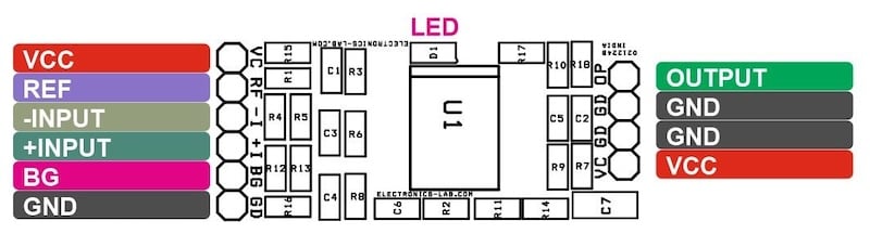
Figure 3. Connection diagram for the Instrumentation Amplifier with Bias Current Cancellation.
CN1 — Power and Output Header (4-pin, 2.54 mm pitch):
- Pin 1 = VCC
- Pin 2 = GND
- Pin 3 = GND
- Pin 4 = Output
CN2 — Input Header (6-pin, 2.54 mm pitch):
- Pin 1 = VCC
- Pin 2 = Reference Input
- Pin 3 = -Input
- Pin 4 = +Input
- Pin 5 = NC/BG
- Pin 6 = GND
D1 — Power LED
PCB Files
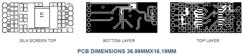
Figure 4. PCB layout showing the silkscreen, top layer, and bottom layer. Board dimensions are 36.99 mm x 16.19 mm.
You can download the layout files for this project here:
Instrumentation Amplifier with Bias Current Cancellation Gerber Files
All images used courtesy of Rajkumar Sharma
Related Content