 Facebook
 Google
 GitHub
 Linkedin
How to Add Bluetooth 5 to a Project with a GT-tronics BLE5 Module
This article demonstrates a solderless-breadboard compatible carrier-board for a pre-certified BLE4 or BLE5 module made by GT-Tronics. Use it to experiment with your own BLE5 compatible designs.
If you're looking experiment with your own BLE5 compatible designs, this project is for you. This article demonstrates a solderless-breadboard compatible carrier-board for a pre-certified BLE4 or BLE5 module made by GT-Tronics.
As Bluetooth Low Energy 5.0 (BLE5) continues to enter the market, you will undoubtedly want to start incorporating it into your next design. BLE5.0 remains backward-compatible with previous BLE standards and adds two new PHY layers: long distance (LE 1M coded), which supports link distances of 1.5 km at decreased data rates, and high speed (LE 2M).
While very large-scale operations can afford to design custom modules or boards and have them FCC certified, most designers incorporating BLE5 will have to make do with pre-certified modules from secondary manufacturers.
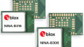
This project makes a carrier board for FCC-certified BLE4 or BLE5 modules made by GT-tronics. GT-tronics uses the Texas Instruments CC2640 SoC on their CC264BNA-S module, which we'll use in this design. Complete board files are available at the end of the article.
This design incorporates the CC264BPA-S module, the Silicon Labs CP2102N USB-to-UART converter, and a 0.1” header to allow interface to a solderless breadboard for prototyping.

Shown above is the carrier board used in this project connected to a solderless breadboard along with a power supply and sensor.
CP2102N USB-to-Serial Converter

The CP2102N USB-to-UART converter from Silicon Labs is a programmable drop-in replacement for their last generation of CP210x chips. The circuit is relatively straightforward in this design.
C4-C7 provide smoothing and decoupling for the input supply and the 3.3 V rail generated by the chip’s internal regulator. R9 is a pull-up resistor that enables the IC. No hardware reset was utilized in this design as it was not required. TP RXD and TP TXD are plated through-hole test points for use during testing.
The USB connection is through a Micro-B connector; the shield is connected to data ground through a zero-ohm resistor. This part can be replaced with a different passive component if you’re having ground-loop or EMI issues. ESD protection for the data lines is provided by diode array D3.

Schematic and PCB implementation for the USB interface circuit
The USB differential-pair data lines are routed to the opposite side of the board through a single pair of vias. If the connector and the CP2102N are on the same side of the board, the USB data lines must cross each other to correctly connect to the CP2102N, and the only way to do that is to move a portion of one differential-pair trace to a different board layer.
The better solution is to place the connector and CP2102N components on opposite sides of the board and to connect both traces with vias.

Ranked in order of descending design preference from left to right: no vias, traces that enter and exit board layers at ends of vias, one trace that crosses another using two vias and an external board layer, vias with traces entering/exiting at intermediate board layers.
Since the CP2102N is used to provide power for the rest of the circuit, thermal vias must be placed on the exposed pad to thermally connect the die to the ground layer and/or copper pours for heat dissipation.

This animation shows the location and proximity of the USB connector, the ESD diode array, and the thermal vias for the CP2102N.
Two LEDs are incorporated into this design to indicate UART activity between the CP2102N and the CC264BPA module. The reverse-mount LEDs are not strictly necessary but are included due to a surplus left over from a previous design (the capacitive control panel PCB). To enable the Tx/Rx LED indicators, the CP2102N must be programmed through the Silicon Labs Simplicity Studio Xpress Configurator utility.
The fields that must be changed are under the grouping “Port Configuration: GPIO”. GPIO0 alternate function should be changed to “TX Toggle”, and GPIO1 alternate function should be changed to “RX Toggle”.

To enable the TX/RX LEDs, use the Silicon Labs XPress Configuration utility. Create a custom serial number to avoid future problems with USB3.0 serial port enumeration on Windows.
The CC264BPA-S Module
The CC264BPA-S is the RF shielded module from GT-tronics (though a non-shielded version is available, as well). This module is based on the CC2640 SoC from Texas Instruments. The CC2640 supports cTag and JTAG programming.
The least expensive way to program it is with a modified XDS110 DevPackDebug tool from TI. It will plug directly into the JTAG header on the carrier board. Details on modifying the DevPackDebug tool are available in a previous article on adding Bluetooth capabilities to a project, but all you have to do is add a single wire to provide 3.3 V to the JTAG header on pin 1.

Left: A pinout diagram (pertinent pins only) for the TI XDS Debugger Devpack. Center: An XDS110 Debugger Devpack with wires connected for 3.3 V power and ground. Right: An optional connection between 3.3 V power (pin 1 of the through holes) to pin 1 of the JTAG debug probe (click image to enlarge)
Programming the CC264BPA Module
Texas Instruments released the CC2640R2F128 (BLE5.0) after the CC2640F128 (BLE4.1) and, since the newer chip can do everything the original chip could do, the original CC2640F128 (BLE4.1) has fallen from favor. GT-Tronics has discontinued manufacturing of the BLE4.1 variant, and now only ships the BLE5.0 version. They used identical footprints, so no changes to the board file are necessary.
After connecting the modified debug tool (or a proper XDS110 probe), you can use the Texas Instruments SmartRFFlash Programmer 2 to immediately connect and read the memory of the device to a file, as well as verify which chip you have in your module (CC2640 or CC2640R2). This program also provides the ability to write that file back to memory and thus restore to a factory default state if you happen to brick it later on.
Code Composer Studio 8 (CCS8) was recently released and is the IDE that TI suggests for developing your code. To begin, you have to download, install, and then further modify the CCS8 installation to work with the GT-tronics module.
A complete walkthrough for version 7 of CCS that is appropriate for the CC2640F128 module (BLE4) is available here; this walkthrough should work for version 8, as well (but if you have any issues, please leave a comment and let us know). An updated guide for modifying your installation for the CC2640R2F128 module (BLE5) is available here.
The modifications for BLE4 and BLE5 are different. Use the guide that is appropriate for your module (likely BLE5)
Serial Bootloader
The CC2640 modules can be programmed via serial-port (or USB-to-serial) communication after enabling the serial bootloader configuration flags in the memory at address 0x0001.FFD8.
Beginning with memory address 0xFD8, write the values C5, 07, FE, and C5. The first C5 flags on either end enable the functionality. The pin number checked during power-on reset (POR) is 0x07, to correspond to DIO_7 on the carrier board.
The next bit determines the logic level that, when applied to the selected pin, will place the device in Serial Bootloader Mode.

For this particular carrier board, the values 0xC5, 0x07, 0xFE, 0xC5 should be written to memory addresses 0x0001.FFD8 to 0x001.FFDB.
Note for readers: The datasheet uses the period in the hex address, but the SmartRF Flash Programmer 2 does not.

Use the Texas Instruments Flash Programmer 2 to read, change, and then write the values C5, 07, FE, C5 to memory locations beginning with 0x0001.FFD8.
Once those locations in memory have been overwritten with the new values, you can put away the XDS110 debug tool, as the device can now be programmed over USB.
USB Programming
The CC2538/CC26xx serial bootloader interface datasheet that details the Serial Bootloader Entry Sequence, along with source code and precompiled binaries, are available from Texas Instruments; the information in these documents will help you to successfully program the CC2640 using a variety of platforms.
You should not start loading binary files built for the TI LaunchXL-CC2640R2 or CC26xBPA-TIEM over USB without compiling them yourself, as you can overwrite the memory location 0xFD9 (which controls the SBL entry pin) and thereby prevent the upload of any other firmware over USB. Then it’s back to the XDS110 for correction.

Circuit Characteristics
I used the AVHzY USB power meter to determine the current consumption of the board at various stages of construction. Before the addition of the Bluetooth module, the current consumption of the board surges to 8.4 mA while the device is interrogated by the computer, and then settles back to 410 µA.
The CP2102N datasheet indicates that the normal current consumption is ~9.5–13.7 mA (depending on communication speed) and the suspend current consumption is 195 µA. The datasheet values are reasonably close to the measured values, and any discrepancies might be attributed to inevitable differences in circuit details and test conditions.
The addition of the CC264BPA module (programmed with a simple UART echo program and not transmitting BLE) indicated slightly higher values: 11.73 mA during UART communication, and 3.34 mA during idle.
Now we can try a test. Check out my video below:
Conclusion
My PCB has 10 GPIO pins as well as two GND pins, a 5 V input pin (tied to USB VBUS), and a 3.3 V output pin all connected to a 14-pin 0.1” male header for direct plug into a solderless breadboard. Power can be supplied to the board through USB or the 5 V input pin (not both).
This board provides a USB programming and debugging interface to BLE4.0/BLE5.0 module from GT Tronics that is based on Texas Instruments CC2640 SOC. Use it to experiment with the new PHY layers and let us know in the comments what you build.


nice project