Facebook
 Google
 GitHub
 Linkedin
A 7 to 60 V Input Buck Converter: A Wide-Range DC-DC Step-Down Module
This project brief describes how to build a wide-range DC-DC buck converter capable of delivering a regulated 5.0 or 3.3 V output from input voltages ranging from 7 to 60 V.
This compact buck converter module accepts input voltages from 7 V to 60 V DC and steps them down to either 5.0 or 3.3 V. The output voltage is selectable via a jumper. The assembled module is shown in Figure 1.
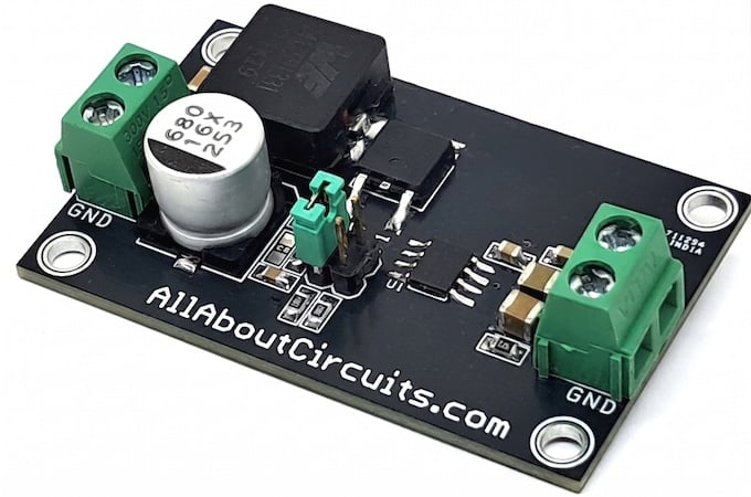
Figure 1. Assembled 7 to 60 V Input Buck Converter module.
The heart of the design is the ROHM BD9G500UEFJ-LA, an 8-pin SMD buck converter IC with an integrated high-side power MOSFET featuring low on-resistance. The device operates in current-mode control and can supply continuous output currents up to 5 A, with a nominal rating of 2 A for typical use.
The BD9G500UEFJ-LA operates at a fixed switching frequency of 200 kHz, set by the RT resistor. Current-mode control provides inherently fast transient response and simplifies the phase-compensation network. The output voltage is programmed by the feedback resistor divider (R3/R4 for 5 V, R3/R5 for 3.3 V) connected to the FB pin, and the appropriate setting is selected by placing the shunt jumper on J1 (5 V) or J2 (3.3 V).
The module includes a Schottky catch diode (D1, RB088BM100TL), a 33 µH power inductor (L1), and a bulk output capacitor (C5, 220 µF/50 V). Input decoupling is provided by C3 and C4 (10 µF/100 V ceramic, 1210 package), with additional high-frequency filtering on the boot and bias rails. Screw terminal connectors (CN1, CN2) are used for both the input supply and the output load connection.
Specs and Features
- Input supply range: 7 to 60 V DC (76 V absolute maximum)
- Output voltage: 5.0 V or 3.3 V, selectable via jumper (J1/J2)
- Output current: 2 A nominal, 5 A maximum
- Switching frequency: 200 kHz
- Control architecture: current-mode
- Soft-start function to limit inrush current and output overshoot
- Over-current protection (OCP): auto-restart after 4 consecutive events
- Under-voltage lockout (UVLO): 6.4 V threshold, 200 mV hysteresis
- Over-voltage protection (OVP) with integrated discharge MOSFET
- Thermal shutdown (TSD): 175°C, 25°C hysteresis
- Enable control via EN pin (2.5 Von, 0.4 Voff)
- PCB dimensions: 53.34 × 32.86 mm
- Mounting holes: 4 × 2.5 mm
How It Works
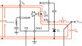
The BD9G500UEFJ-LA is an 8-pin synchronous buck controller with an integrated high-side MOSFET. On each switching cycle, the internal MOSFET connects VIN to the SW node, energizing inductor L1 and delivering current to the output. When the MOSFET turns off, the catch diode D1 provides a freewheeling path, and the inductor current continues flowing to the load. The output voltage is set by a resistor divider from the output to the FB pin. The IC regulates to maintain FB at 0.8 V. A simplified application schematic is shown in Figure 2.
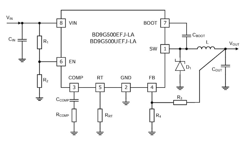
Figure 2. BD9G500UEFJ-LA buck converter topology. Image used courtesy of Rohm Semiconductor
Current-mode control senses the high-side MOSFET current every cycle. If an overcurrent condition occurs, the cycle is skipped. After four consecutive OCP events, the converter stops for 20 ms (typical) before attempting a restart.
During start-up, the soft-start circuit ramps the duty cycle slowly to prevent inrush current and output voltage overshoot. The RT resistor (C7, 6.8 kpF in this design) sets the switching frequency to 200 kHz. The COMP pin and its associated RC network set the loop compensation bandwidth.
Under-voltage lockout prevents operation below 6.4 V on VIN, protecting against brownout conditions. Thermal shutdown activates at a die temperature of 175°C and resets once the temperature drops by 25°C.
Over-voltage protection monitors the FB pin. When FB exceeds 1.2 V (Typ), the high-side MOSFET is disabled, and the integrated discharge MOSFET helps pull the output down. The enable pin (EN) allows the converter to be turned on and off by an external logic signal, requiring a minimum low interval of 100 µs for a valid shutdown.
Schematic and Bill of Materials
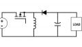
Figure 3 shows the schematic for the buck converter design.
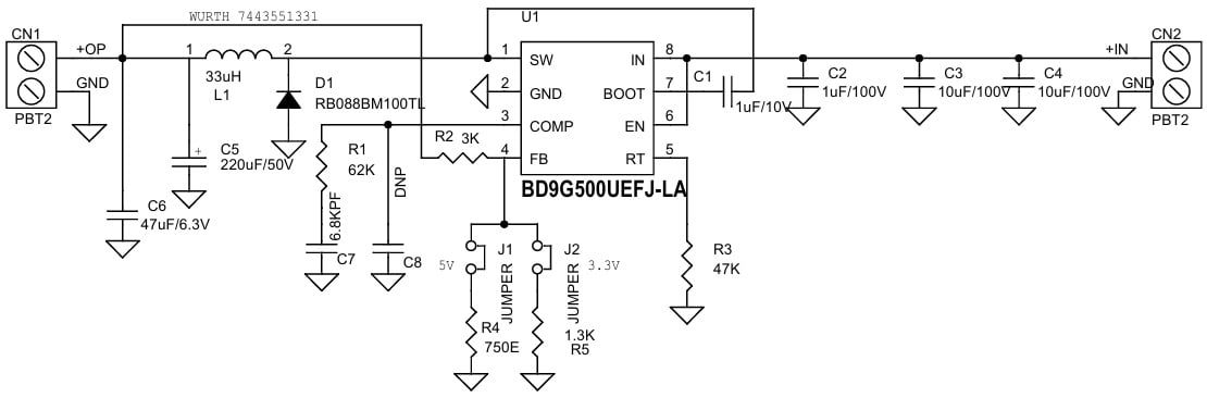
Figure 3. Complete schematic for the 7V to 60V Input Buck Converter.
The bill of materials is shown in Table 1.
Table 1. BOM for the 7 to 60 V Input Buck Converter.
| REF | DESCRIPTION | QTY | MFG | SUPPLIER | PART NO. |
| CN1, CN2 | 2 Pin Screw Terminal, 5.08 mm Pitch | 2 | Phoenix | DigiKey | 277-1247-ND |
| C1 | 1 µF/10 V Ceramic SMD 0805 | 1 | Yageo/Murata | DigiKey | |
| C2 | 1 µF/100 V Ceramic SMD 0805 | 1 | Yageo/Murata | DigiKey | |
| C3, C4 | 10 µF/100 V Ceramic SMD 1210 | 2 | Yageo/Murata | DigiKey | |
| C5 | 220 µF/50 V Electrolytic 10.3×10.3 mm | 1 | Nichicon | DigiKey | 493-2308-1-ND |
| C6 | 47 µF/6.3 V Ceramic SMD 0805 | 1 | Yageo/Murata | DigiKey | |
| C7 | 6.8 kpF/50 V Ceramic SMD 0805 | 1 | Yageo/Murata | DigiKey | |
| C8 | DNP | 1 | |||
| D1 | RB088BM100TL Schottky Diode | 1 | ROHM | DigiKey | 846-RB088BM100TLCT-ND |
| J1, J2 | 2-Pin Male Header, 2.54 mm Pitch | 2 | Würth | DigiKey | 732-5315-ND |
| L1 | 33 µH Inductor, 13×12.5 mm | 1 | Würth | DigiKey | 732-3881-1-ND |
| R1 | 62 kΩ 1% SMD 0805 | 1 | Yageo/Murata | DigiKey | |
| R2 | 3 kΩ 1% SMD 0805 | 1 | Yageo/Murata | DigiKey | |
| R3 | 47 kΩ 1% SMD 0805 | 1 | Yageo/Murata | DigiKey | |
| R4 | 750 Ω 1% SMD 0805 | 1 | Yageo/Murata | DigiKey | |
| R5 | 1.3 kΩ 1% SMD 0805 | 1 | Yageo/Murata | DigiKey | |
| U1 | BD9G500UEFJ-LA Buck Converter IC | 1 | ROHM | DigiKey | 846-BD9G500UEFJ-LAE2CT-ND |
| J1, J2 | Shunt | 1 | Sullins Connector | DigiKey | S9001-ND |
Connections
Figure 4 shows the connection diagram. Refer to the descriptions below for each connector.
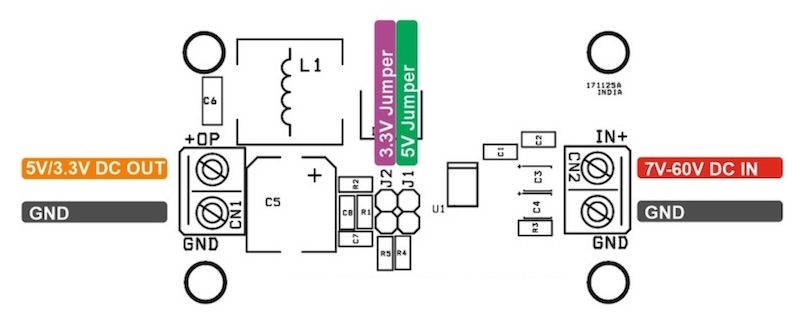
Figure 4. Connection diagram for the 7 to 60V Input Buck Converter.
CN1 — Output Connector (2-pin screw terminal, 5.08 mm pitch):
- Pin 1 (+OP) = 5.0 or 3.3 V DC Output
- Pin 2 (GND) = Ground
CN2 — Input Connector (2-pin screw terminal, 5.08 mm pitch):
- Pin 1 (IN+) = 7 to 60 V DC Input
- Pin 2 (GND) = Ground
J1 — 5 V Output Selection Jumper (2-pin header, 2.54 mm pitch):
- Install a shunt to select a 5 V output
J2 — 3.3 V Output Selection Jumper (2-pin header, 2.54 mm pitch):
- Install shunt to select 3.3 V output
Note: Install only one jumper shunt at a time. Installing both simultaneously will result in undefined output behavior.
PCB Files
Figure 5 shows the silk screen, bottom, and top layers. The board dimensions are 43.34 × 32.86 mm. The Gerber files for fabrication are available for download below.
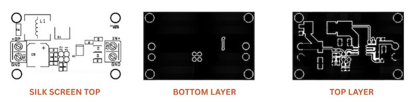
Figure 5. PCB layout: silk screen top, bottom layer, and top layer.
7 to 60 V Input Buck Converter Gerber Files
You can download the layout files for this project here:
Except where noted, all images used courtesy of Rajkumar Sharma.
Related Content