 Facebook
 Google
 GitHub
 Linkedin
How to Design a Bilateral RF Amplifier for Maximum Gain
This article explores the design of bilateral RF amplifiers for maximum transducer gain, and explains how to assess whether an RF amplifier is bilateral or unilateral.
Different RF amplifiers have different performance requirements. For example, achieving maximum output power might be a major concern for a power amplifier located at a transmitter output, but designs for low-noise amplifiers (LNAs) placed at the front end of an RF receiver will likely focus on providing an acceptable level of power gain with the minimum possible noise. Other amplification stages that appear after the LNA might be designed for maximum gain.
In the previous article in this series, we learned how to design a unilateral RF amplifier for a specified gain. In this installment, we’ll focus on designing bilateral RF amplifiers for maximum transducer gain. First, however, we’ll learn how to determine if a device is bilateral.
Unilateral Figure of Merit
With a unilateral device, the gain of the input and output matching sections can be set independently, which significantly simplifies the design equations. In practice, transistors aren’t perfectly unilateral, but with a sufficiently small S12 we might still be able to use the unilateral approach without incurring significant error.
But what qualifies as a “sufficiently small” S12? We can use the unilateral figure of merit (U) to assess whether the reverse gain of the transistor is negligible. The unilateral figure of merit is given by:
$$U~=~\frac{|S_{12}||S_{21}||S_{11}||S_{22}|}{(1~-~|S_{11}|^2)(1~-~|S_{22}|^2)}$$
Equation 1.
Note that U is a function of all the S-parameters, not just S12. As such, U is also frequency-dependent.
When we ignore the reverse gain of the transistor and assume that S12 = 0, we are approximating the amplifier’s actual transducer gain (GT) by its unilateral transducer gain (GTU). By showing how the ratio of these two gain terms is related to U, Equation 2 allows us to estimate the difference between the computed unilateral gain obtained by approximating S12 as zero and the actual gain the circuit exhibits.
$$\frac{1}{(1~+~U)^2}~<~\frac{G_T}{G_{TU}}~<~\frac{1}{(1~-~U)^2}$$
Equation 2.
Because of this relationship to U, all of the S-parameters can play a role in the magnitude of error when S12 ≠ 0. Figure 1 provides a log-log plot of the error in dB against the unilateral figure of merit.
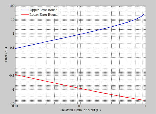
Figure 1. Error of the unilateral gain computations vs. the unilateral figure of merit. Image used courtesy of Steve Arar
We can see that the error increases rapidly as U becomes greater, so it might not be a good idea to use the unilateral approximation for higher values of U. However, if U is less than 0.1, the error of the unilateral method is less than about ±1 dB. When the transistor is unilateral (S12 = 0), Equation 1 produces U = 0, making the transducer gain equal to the unilateral transducer gain (zero error).
Example 1: Calculating Error
Figure 2 plots the unilateral figure of merit versus frequency for a transistor with a small but non-zero S12. If we approximate S12 as zero, how much will the actual gain differ from the designed unilateral gain?
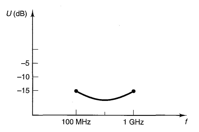
Figure 2. Unilateral figure of merit vs. frequency for a transistor with a small, non-zero S12. Image used courtesy of G. Gonzalez
The above figure shows that U is less than –15 dB (or 0.03, in linear terms). Using Equation 2, we can find the exact value of the error bound; alternatively, we can use Figure 1’s plot of the equation as a graphical solution. According to Figure 1, the error of the unilateral method in this case is less than ±0.3 dB.
It’s worth mentioning that Equation 2 only gives us the worst-case error. The actual error can be much smaller. Even when that’s the case, the equation is still very useful—it helps us to quickly find the limits for the maximum error.
The Bilateral Design Method
When the error of the unilateral approach is intolerably large, it’s necessary to use the bilateral design method, which can account for the transistor’s reverse gain. Consider the basic single-stage amplifier in Figure 3.
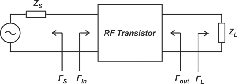
Figure 3. Single-stage amplifier. Image used courtesy of Steve Arar
The amplifier has the S-parameters of its component transistor, so its performance is a function of its source and load terminations (ΓS and ΓL). With the unilateral approach, we would simply set ΓS = S11* and ΓL = S22* to obtain the maximum gain. When the transistor is bilateral, we still need to provide a simultaneous conjugate match at both input and output ports to have the maximum gain, so that:
$$\Gamma_S~=~\Gamma_{IN}^*~~~~\text{and}~~~~\Gamma_L~=~\Gamma_{OUT}^* $$
Equation 3.
ΓIN is calculated as:
$$\Gamma_{IN}~=~S_{11}~+~\frac{S_{12}S_{21} \Gamma_L}{1~-~S_{22}\Gamma_L}$$
Equation 4.
and ΓOUT, as:
$$\Gamma_{OUT}~=~S_{22}~+~\frac{S_{12}S_{21} \Gamma_S}{1~-~S_{11}\Gamma_S}$$
Equation 5.
What makes the bilateral design more complicated is that there’s an interaction between the input and output ports of a bilateral device. As a result, the two conditions provided in Equation 3 are coupled, and the two expressions in Equation 3 must be solved simultaneously to find the appropriate ΓS and ΓL.
The unilateral design for maximum gain is actually a special case of the bilateral method where S12 is set to zero, decoupling the input and output equations and simplifying ΓIN and ΓOUT to S11 and S22, respectively.
The ΓS and ΓL for simultaneous conjugate match in a bilateral amplifier can be found using the following two equations:
$$\Gamma_S~=~\frac{B_1~-~\sqrt{B_{1}^{2}~-~4|C_1|^2}}{2C_1}$$
Equation 6.
and:
$$\Gamma_L~=~\frac{B_2~-~\sqrt{B_{2}^{2}~-~4|C_2|^2}}{2C_2}$$
Equation 7.
B1, B2, C1, and C2 are given by:
$$B_1~=~1~+~|S_{11}|^2~-~|S_{22}|^2~-~|\Delta|^2 $$
Equation 8.
$$B_2~=~1~+~|S_{22}|^2~-~|S_{11}|^2~-~|\Delta|^2 $$
Equation 9.
$$C_1~=~S_{11}~-~\Delta S_{22}^*$$
Equation 10.
$$C_2~=~S_{22}~-~\Delta S_{11}^*$$
Equation 11.
and Δ, the determinant of the scattering parameters matrix, is calculated as follows:
$$\Delta~=~S_{11}S_{22}~-~S_{12}S_{21}$$
Equation 12.
The above equations are valid for unconditionally stable devices. An unconditionally stable device can always be conjugately matched for maximum gain. If the device is potentially unstable, we can stabilize it and then find the terminations for the simultaneous conjugate match condition. The maximum transducer gain (GT,max) for a simultaneously conjugate matched device is given by:
$$G_{T, max}~=~\frac{|S_{21}|}{|S_{12}|}~\times~(K~-~\sqrt{K^{2}~-~1})$$
Equation 13.
where K, the stability factor, is:
$$K~=~\frac{1~-~|S_{11}|^2~-~|S_{22}|^2~+~|\Delta|^2}{2|S_{12}S_{21}|}$$
Equation 14.
Maximum Stable Gain
Maximum stable gain (MSG) is defined as the value of GT,max for K = 1. From Equation 13, we have:
$$G_{MSG}~=~\frac{|S_{21}|}{|S_{12}|}$$
Equation 15.
K = 1 represents borderline stability, and GMSG is the gain we achieve after stabilizing a potentially unstable device to that point. This gain quantity allows us to compare the gain of different devices under stable operation conditions. Transistor datasheets normally provide GT,max at frequency points where the transistor is stable, and GMSG at frequencies where the device is potentially unstable. The datasheets usually also provide this information as a plot of the GMSG and GT,max versus frequency, like the one in Figure 4.
Note that under simultaneous conjugate match conditions, the available gain (GA) and the transducer gain (GT) are equal. In Figure 4, this gain term is labeled as MAG (maximum available gain). The plot suggests that the device is potentially unstable below about 1.5 GHz.
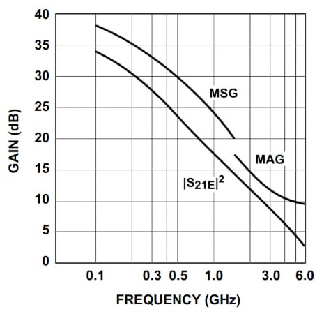
Figure 4. Typical MAG (GA,max or GT,max) and MSG curves from an RF transistor datasheet. Image used courtesy of Hewlett-Packard
In practice, the achievable MSG can be 2 to 3 dB less than what’s provided by Equation 15. This is because practical designs don’t use the device in the borderline of stability—instead, they slightly over-stabilize it. Another reason for this reduced practical gain is the unavoidable losses from the components used in matching networks, etc.
Example 2: Calculating Maximum Transducer Gain
Assume that Z0 = 50 Ω for a transistor with the S-parameters tabulated below.
Table 1. S-parameters for an example transistor.
| f (GHz) | S11 | S21 | S12 | S22 |
| 0.8 | 0.440 ∠ –157.6 | 4.725 ∠ 84.3 | 0.06 ∠ 55.4 | 0.339 ∠ –51.8 |
| 1.4 | 0.533 ∠ 176.6 | 2.800 ∠ 64.5 | 0.06 ∠ 58.4 | 0.604 ∠ –58.3 |
| 2.0 | 0.439 ∠ 159.6 | 2.057 ∠ 49.2 | 0.17 ∠ 58.1 | 0.294 ∠ –68.1 |
Our goal is to determine the maximum transducer gain for f = 1.4 GHz. We’ll do this by finding the ΓS and ΓL values for the simultaneous conjugate match condition at this frequency.
First, let’s see if we can consider the device unilateral. If we use Equation 1 to calculate the unilateral figure of merit at f = 1.4 GHz, we get a value of U = 0.12. This means that the error from the unilateral approximation is relatively large, and we need to apply the bilateral method.
Next, we need to verify that the transistor is unconditionally stable. To do this, we use Equations 12 and 14 to calculate Δ and K; if |Δ|< 1 and K is greater than unity, the device is unconditionally stable at that frequency. At f = 1.4 GHz, the transistor does turn out to be unconditionally stable, so we can find ΓS and ΓL values that satisfy the simultaneous conjugate match conditions. If the transistor were unconditionally stable only at f = 1.4 GHz, we could still use our bilateral design equations, but we would have to check that the obtained ΓS and ΓL values are in the stable region of operation at all frequencies. However, you can verify that this transistor is unconditionally stable for all three of the frequencies in Table 1.
Another option with a potentially unstable device is to first stabilize the device, then apply the bilateral design equations to the newly stable device’s S-parameters. Applying Equations 6 and 7 at f = 1.4 GHz, we obtain ΓS = 0.83 ∠ –177.66 and ΓL = 0.85 ∠ 57.51. Substituting K = 1.12, |S21|=2.8, and |S12|=0.06 into Equation 13 gives us a maximum transducer gain of GT,max = 28.73, which translates to 14.58 dB. The matching networks can easily be determined using a Z Smith chart.
For the input matching section, we locate ΓS on the Smith chart and find its associated normalized admittance (yS) through a 180 degree rotation along the constant |ΓS| circle. The point yS has a normalized admittance of approximately 10 + j2, as shown in Figure 5.
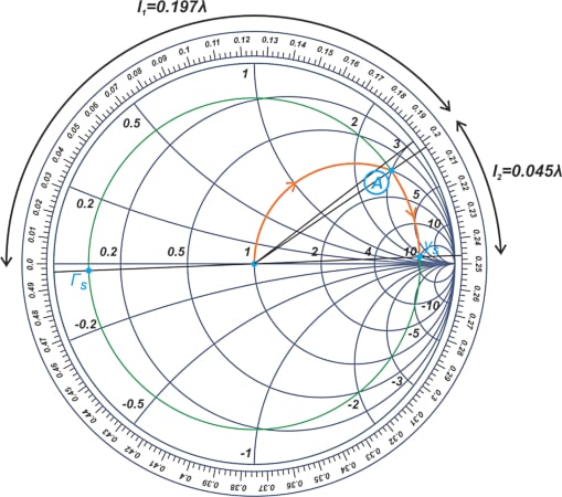
Figure 5. Smith chart showing the constant ΓS circle for an example transistor. Image used courtesy of Steve Arar
From now on, we interpret the Smith chart as a Y Smith chart. We want a circuit that takes us from the center of the chart (or the 50 Ω termination) to yS. The intersection point of the constant |ΓS| circle with the (1 + jB) circle is marked as point A, and has a susceptance of j3.
To create this susceptance, we add a parallel, open-circuited stub of length l1 = 0.197λ to the 50 Ω termination. We then add a series line of length l2 = 0.045λ to travel along the constant |ΓS| circle to yS. The output matching section can be designed in a similar way; the Smith chart in Figure 6 shows the details.
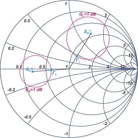
Figure 6. Smith chart showing the constant ΓL circle for an example transistor. Image used courtesy of Steve Arar
Figure 7 shows the final input matching section. As you can see, we need an open-circuited stub of length l3 = 0.203λ and a series line of length l4 = 0.214λ.
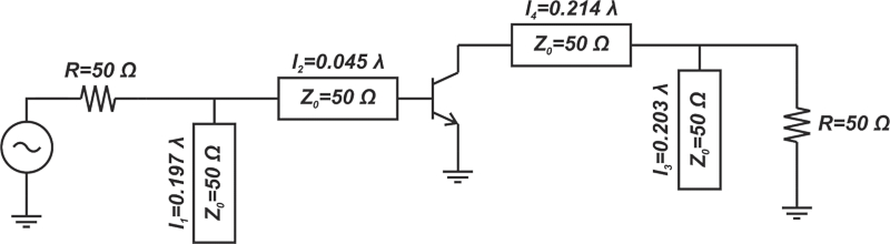
Figure 7. The RF amplifier’s input matching section. Image used courtesy of Steve Arar
Figure 8 shows the simulated gain of the amplifier, which is very close to the calculated value of GT,max = 14.58 dB.
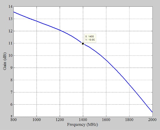
Figure 8. Simulated gain of an example RF amplifier. Image used courtesy of Steve Arar
Figure 9 shows the amplifier’s input reflection coefficient. The input is well matched to the 50 Ω source impedance.
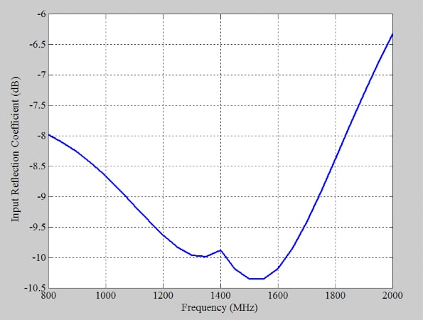
Figure 9. The amplifier’s input reflection coefficient. Image used courtesy of Steve Arar
In the above simulations, the software was provided with the S-parameters at 0.8, 1.4, and 2 GHz. The S-parameters for any other required frequency points can be obtained through interpolation.
Summary
We’ve covered a lot of material in this article. Below are the major takeaways:
- The unilateral figure of merit U allows us to assess whether or not the reverse gain of the transistor is negligible.
- If U is less than 0.1, the error of the unilateral method is less than about ±1 dB.
- For higher values of U, it is recommended to use the bilateral design which accounts for the interaction between the input and output ports of the device.
- An unconditionally stable device can always be designed for simultaneous conjugate matched which maximizes the gain.
- If the device is potentially unstable, we can use stabilization techniques to stabilize the device and then find the terminations for the simultaneous conjugate match condition.
Featured image used courtesy of Adobe Stock


complex!