 Facebook
 Google
 GitHub
 Linkedin
How to Design Charge Amplifiers for Piezoelectric Sensors
This article explores charge-amplifier design details, including ESD protection and frequency response.
This article explores charge-amplifier design details, including ESD protection and frequency response.
Related Information
- An Introduction to Motion Sensors: PIR, Tilt, Force, and More
- How Piezoelectric Speakers Work
- Understanding and Modeling Piezoelectric Sensors
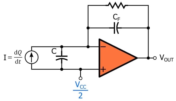
In a previous article, I presented the charge amplifier as an effective way to convert the charge generated by a piezoelectric sensor into a normal voltage signal. A charge amplifier uses the basic integrator topology—i.e., a capacitor in the feedback path produces an output voltage that is proportional to the integral of the input current, and a resistor in the feedback path prevents the amplifier from saturating.
Single-Supply Systems
The output voltage will extend above and below the voltage connected to the noninverting input terminal. If you have a negative supply rail for your op-amp, you can ground this terminal; if you’re using a single-supply system, you’ll often need to provide a bias voltage. In the diagram above, the bias voltage is VCC/2. This is a logical choice, because when no input signal is present the output will be in the middle of the supply range, and consequently the voltage available for positive and negative signal swing is maximized.
However, VCC/2 is by no means an appropriate choice for every design. If you know that your output signals will have more positive deviation than negative deviation, you could choose a bias voltage that is closer to ground. For example, I once designed an amplifier circuit in which the input signal was a pulse-shaped positive excursion, but the AC coupling preceding the amplifier resulted in a small negative excursion at the end of the pulse. If I recall correctly, I used a 3.3 V supply voltage and a 0.5 V bias voltage. The 0.5 V bias was enough to preserve the characteristics of the negative excursion, and the dynamic range for the positive excursion was significantly higher than what I would have obtained by using a bias voltage of VCC/2.
Input Resistance
The circuit shown above can benefit from input resistance placed between the piezoelectric sensor and the inverting input terminal:
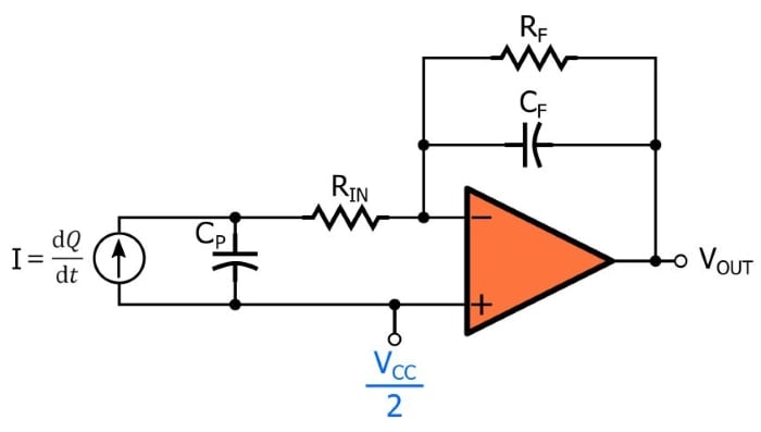
This resistor protects the op-amp by limiting the amount of current generated by whatever voltage might be connected to the inverting input terminal. We certainly are not expecting dangerous voltages from the piezoelectric sensor; rather, the concern here is faults such as an ESD strike. If you’re operating in a benign environment and you’re careful about grounding yourself as you are working with sensitive components, you probably don’t need to worry about destructive currents. But sensors are often used in industrial environments where hazardous electrical conditions are commonplace, and in these circumstances it makes sense to include protective circuitry.
Even if you don’t need RIN as a protection component, you should still consider including it in your circuit. An AAC contributor explained to me that a resistor connected between the sensor and the inverting input terminal can prevent problems associated with amplitude peaking or even oscillation at high frequencies. He recommends a resistance somewhere in the 100 Ω to 1 kΩ range.
Frequency Response
The idealized integrator—i.e., the version that has only a capacitor in the feedback path and no input resistor—exhibits the same behavior at low, medium, and high frequencies. As soon as we start adding resistors, though, we have to consider the circuit’s frequency response.
Attenuation of Low Frequencies
The feedback resistor RF makes the circuit behave like a high-pass filter at low frequencies. The cutoff frequency is calculated as follows:
$$F_{HP}=\frac{1}{2\pi R_FC_F}$$
The feedback resistor does not affect the gain. Thus, you choose the CF value according to the system’s required gain, then you identify an RF value that creates an appropriate frequency response. The trade-off here is low-frequency gain vs. the resistor’s ability to discharge the capacitor and provide a dc bias-current path for the inverting input terminal. You can see from the equation that a lower resistance for RF creates a higher cutoff frequency, meaning that lower-frequency sensor signals will be attenuated. This is why the value chosen for RF is typically very large—1 MΩ is probably a good place to start, with adjustments down toward 100 kΩ or up toward 10 MΩ according to the required low-frequency performance.
Attenuation of High Frequencies
In the previous article, I pointed out that charge amplification of piezoelectric sensor signals is, in many cases, superior to voltage-mode amplification because the charge amplifier’s gain is not affected by cable capacitance. This situation changes somewhat when we include resistor RIN. The gain in the middle of the frequency range remains independent of cable capacitance, but the resistance in series with the inverting input terminal combines with cable capacitance to create high-frequency roll-off. Thus, we now have a high-pass response (caused by RF) and a low-pass response (caused by RIN).
The following equation gives the low-pass cutoff frequency; note that CP includes the piezoelectric sensor’s internal capacitance, the cable capacitance, and any other capacitance that is in parallel with the sensor.
$$F_{LP}=\frac{1}{2\pi R_{IN}C_P}$$
In most cases this high-frequency roll-off won’t negatively affect the circuit because the cut-off frequency will be well above the frequency range of the physical changes measured by the piezoelectric sensor. However, it’s good to be aware of this effect, and it might be significant if for some reason you have an unusually large amount of input resistance or parallel capacitance.
Understanding Charge-Amplifier Frequency Response
If you attempt to simulate the frequency response of a charge amplifier circuit, you may be confused by the results. For example, I generated the following Bode plot for a circuit with CF = 100 nF, RF = 1 MΩ, RIN = 100 Ω, and CP = 1 nF.
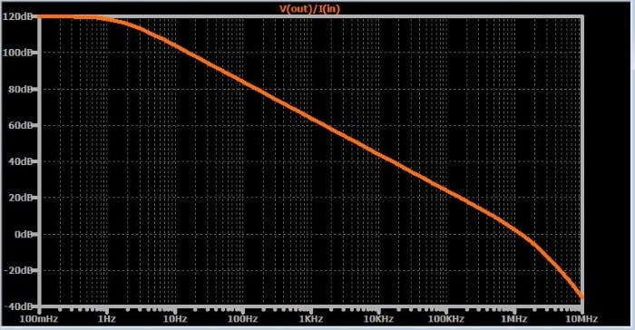
The plot shows no attenuation at low frequencies, a pole around 1 Hz, and a second pole around 1 MHz. These two frequencies make sense given the component values used in the simulation, but the overall behavior isn’t consistent with the frequency response described above. To understand this situation, we have to remember that the magnitude response of the circuit is not identical to the gain response with respect to the circuit’s functionality as an integrator. The frequency response of an ideal integrator corresponds to a line with a uniform slope of –20 dB/decade. Thus, integration occurs at frequencies for which the circuit’s Bode plot has a slope of –20 dB/decade, and as the slope deviates from this value, the circuit’s integrator gain decreases.
Conclusion
We’ve looked at some details involved in the design of charge amplifiers for piezoelectric sensor applications. If you have experience with charge amplifiers and piezoelectric sensors and would like to share some advice, feel free to post a message in the comments section below.


Are there any suggested references for this topology. While integrating amplifier analysis is well covered. I have seen very little as to the frequency response, which as you suggest is a departure from the -20dB/Dec region. Please, could we get some references for this portion of your article?
Thanks
I would like to draw your attention to a couple of (tutorial) articles and book chapters we wrote on Current/charge amplifiers. Feel free to ask copies if you have no access to the journals.
M. Massarotto, A. Carlosena and A. J. Lopez-Martin, “Two-Stage Differential Charge and Transresistance Amplifiers,” in IEEE Transactions on Instrumentation and Measurement, vol. 57, no. 2, pp. 309-320, Feb. 2008.
Charge Amplifiers, A. Carlosena, M. Massarotto, A. J. Lopez-Martin, Encyclopedia of Sensors, IOP, 2006
We designed charge amplifiers, which are inmune to ESD in a harsh environment. They are described in a patent.
Regards