Facebook
 Google
 GitHub
 Linkedin
Creating a Parallel-Load Shift Register in LTspice
We explore the design and functionality of a digital shift register intended for use in mixed-signal circuit simulations.
Like all SPICE derivatives, LTspice is mainly meant for analog simulations. By incorporating logic functions from its digital component directory, however, we can also use it to verify mixed-signal circuits. We examined the structure and simulation behavior of LTspice’s digital components in two previous articles. In this article, we’ll use them to build a parallel-load shift register.
Registers are crucial subcircuits for digital and mixed-signal ICs. In a register, multiple, single-bit memory cells—typically flip-flops—are connected together to form a multi-bit storage device. For example, we’d need the following to make a one-byte register:
- Eight flip-flops.
- Connections that allow us to simultaneously read data from or write data to all eight flip-flops.
What we just described is a basic parallel-input, parallel-output register. In a shift register, we can move digital data from one flip-flop to the next. This feature allows us to convert parallel data into serial data.
For example, say that we load a byte of parallel data into a shift register. We can sequentially shift its component bits through the register’s flip-flops. The last flip-flop in the sequence will then output the original byte as a sequence of eight bits.
An LTspice Shift Register
It would be relatively simple for me to design a shift register that only accepts serial input and produces serial output. The flip-flops would be connected output-to-input, and the input pin of the first flip-flop in the sequence would be the serial input terminal for the entire register. A parallel-load shift register, though much more useful, is also more complex. Its ability to convert parallel data into serial data requires combinational logic to implement a multiplexer function.
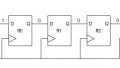
Figure 1 shows the first two flip-flops in my parallel-load shift register. Each flip-flop has the equivalent of a two-to-one multiplexer attached to the input pin.

Figure 1. Two flip-flops, with associated combinational logic, in an LTspice parallel-load shift register.
From this portion of the schematic, you can see:
- The design for each bit of the register.
- How one bit connects to the next bit in the sequence.
I designed this shift register as a four-bit device, though it could easily be expanded to eight or more bits. SPICE software isn’t optimized for simulating digital logic, so there are practical limits on how much digital circuitry you can include in an LTspice schematic. Nevertheless, LTspice handles digital components quite well, and circuits such as the one discussed in this article don’t require long simulation times.
Now that we’re familiar with the shift register’s basic structure, we can take a closer look at its combinational logic.
Important Note: All of the AND and OR gates in this schematic have three unused inputs connected to the common terminal. It’s a peculiarity of LTspice that doing so removes these inputs from the simulation, causing the gates to function as two-input logic gates. For the AND gates, this is NOT the same as tying those inputs to a logic-low input or to ground.
Understanding the Multiplexer Circuit
Let’s go through the function of the shift register’s combinational logic step by step. We’ll use the reference designators shown in Figure 2 for the purpose of this discussion. The other logic blocks have different reference designators but operate in the same way.
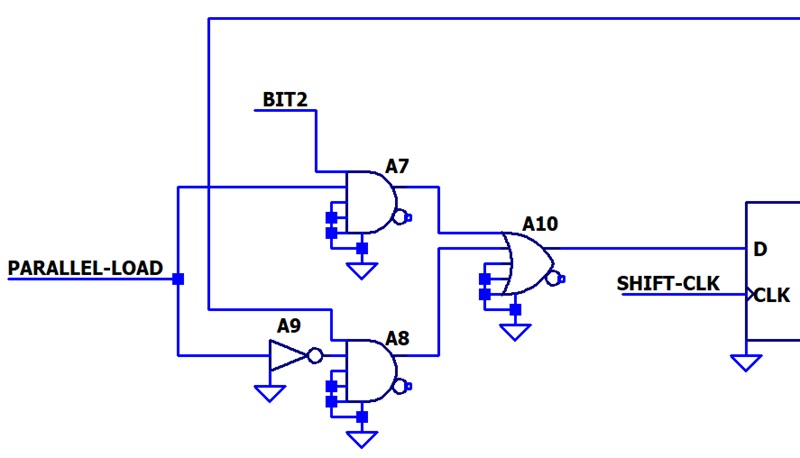
Figure 2. Combinational logic for one flip-flop in the shift register.
The flip-flop has two input signals:
- The primary input is the logic voltage received from the output of the previous flip-flop. It’s connected to the AND gate A8.
- The secondary input is the signal labeled BIT2. It’s connected to the AND gate A7.
The PARALLEL-LOAD signal determines which input signal will be active. For A7, PARALLEL-LOAD is the second of its two input signals; for A8, the second input signal is the inverse of PARALLEL-LOAD. This guarantees that only one of the AND gate outputs can be logic-high at any given moment.
To load parallel data into the register, I set PARALLEL-LOAD high. The AND gate A8’s output is driven to logic-low, and A7 passes the signal BIT2. This BIT2 value then passes through A10 to the D flip-flop’s input, as indicated by the long green arrow in Figure 3.

Figure 3. Signal flow when the register is in parallel-load mode (PARALLEL-LOAD = high).
To operate the register in shift mode, I set PARALLEL-LOAD low. This forces A7’s output to logic-low. As a result, the BIT2 signal is ignored.
Meanwhile, A8’s output reproduces the logic level of the output signal from the preceding flip-flop. The signal passes from A8 to A10, and from A10 to the input of the next flip-flop. The flip-flop’s input now equals the output of the preceding flip-flop. Figure 4 shows the path of this signal.
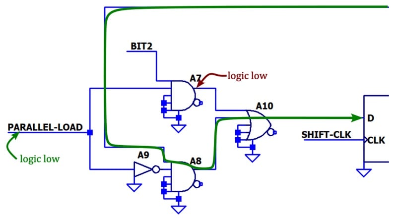
Figure 4. Signal flow when the register is in shift mode (PARALLEL-LOAD = low).
Note that Figure 3 is a synchronous parallel load. When PARALLEL-LOAD is logic-high, the preselected bit value (BIT2) becomes the primary input to the D flip-flop, and the primary input of a D flip-flop is transferred to the output only in response to a transition on the clock. The LTspice D flip-flop is a rising-edge-sensitive device. A successful parallel-load operation therefore requires the PARALLEL-LOAD signal to be active when the clock transitions from logic-low to logic-high.
Wrapping Up
In this article, we looked at the basic structure of the individual bits in an LTspice parallel-load shift register. In the next article, we’ll examine some important schematic details and signal waveforms for this circuit.
All images used courtesy of Robert Keim