 Facebook
 Google
 GitHub
 Linkedin
Digital Design with Pass-Transistor Logic
This article presents efficient, pass-transistor-based implementations of important digital functionality.
This article presents efficient, pass-transistor-based implementations of important digital functionality.
In a previous article, I introduced the concept and basic characteristics of pass-transistor logic (PTL). As the name implies, PTL uses transistors as switches that pass or block a signal; this is in contrast to the “typical” CMOS approach whereby an output node is always driven to logic low or logic high via the low-resistance path provided by a PMOS or NMOS transistor.
The bottom line with pass-transistor logic is that you are trading electrical performance for the possibility of reducing transistor count. The loss in electrical performance is especially disconcerting when the pass/block functionality is provided by an NMOS transistor instead of a CMOS transmission gate (see this article for more information).
The Pass-Transistor AND Gate
In the preceding article, we looked at a two-input AND gate consisting of only one transistor and one resistor. This certainly is a major reduction in component count compared to the typical CMOS two-input AND gate, which requires six transistors. However, we can’t directly compare the NMOS-plus-resistor implementation to the CMOS implementation, because the CMOS version always provides a low-resistance output connection whereas the PTL version does not. If we want a PTL circuit that is more consistent with the functionality of the CMOS circuit, we need an additional transistor:
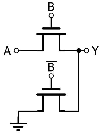
If B is high, the output has a low-resistance path to the supply rail or ground, depending on the state of A (we’re assuming here that the A signal is generated by a low-resistance driver of some kind). If B is low, the upper transistor is in cutoff, but the output is not floating because the lower transistor, which is driven by the complement of B, provides a low-resistance path to ground.
Now we have an AND gate that requires only two transistors instead of six, if the preceding circuitry happens to provide both $$B$$ and $$\overline{B}$$. In the (extremely frequent) situations where $$\overline{B}$$ is not available from the preceding circuitry, it has to be generated by the PTL AND gate, and that requires another two transistors. We’re still ahead—four instead of six.
However, we’re using NMOS transistors here instead of transmission gates. A lone NMOS can effectively transfer a logic-low signal from input to output, but it causes serious signal degradation when it attempts to transfer a logic-high signal. Thus, a more respectable PTL AND gate would look like this:
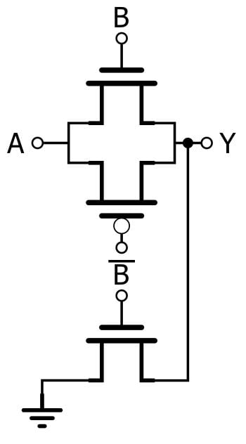
Now we need five transistors, versus six for the standard AND gate. My guess is that IC designers don’t often use PTL for AND gates.
The PTL XOR Gate, Version 1
The XOR function is an example of an application in which PTL really does offer significant benefits. Creating a two-input XOR truth table using typical CMOS logic is a bit awkward—twelve transistors are required, despite the fact that other standard Boolean functions require only four (NAND, NOR) or six (AND, OR). Pass-transistor logic allows us to greatly reduce this transistor count. One of my textbooks has a PTL implementation that requires eight transistors; it consists of two transmission gates and two inverters (one for the A input and one for the B input; the inverters are not shown in the diagram).
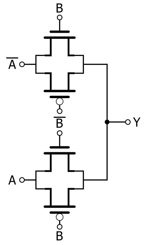
Let’s look at how this circuit works. First, we need to remember the following: A logic-low signal causes an NMOS (indicated by the absence of a circle adjacent to the gate) to turn off and a PMOS (indicated by the presence of a circle adjacent to the gate) to turn on. A logic-high signal causes an NMOS to turn on and a PMOS to turn off. Thus, if a transmission gate has the input signal connected to the NMOS and the complemented input signal connected to the PMOS, it’s an “active high” gate—i.e., it behaves like a closed switch when the input signal is logic high and an open switch when the input signal is logic low. If a transmission gate has the input signal connected to the PMOS and the complemented input signal connected to the NMOS, it is an “active low” gate—it behaves like an open switch when the input is logic high and a closed switch when the input is logic low.
- If B is logic low, the upper transmission gate is blocking its input signal and the lower transmission gate is passing its input signal, meaning that A is passed to the output. Therefore,
- if A is 0 and B is 0, Y is 0;
- if A is 1 and B is 0, Y is 1.
- If B is logic high, the upper transmission gate is passing its input signal and the lower transmission gate is blocking its input signal. In this case, the complement of A is passed to the output. Therefore,
- if A is 0 and B is 1, Y is 1;
- if A is 1 and B is 1, Y is 0.
The PTL XOR Gate, Version 2
When I was doing research for this article, I came across (in these slides) a PTL XOR gate that requires only six transistors. It’s a very clever circuit, and as far as I can tell the performance is equivalent to that provided by the eight-transistor XOR shown above.
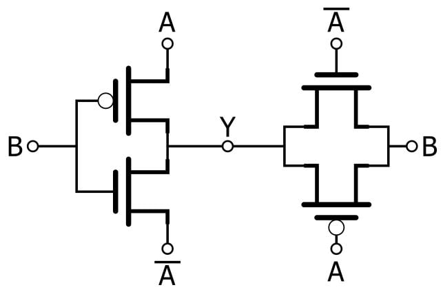
As you can see, the first stage is a standard inverter, and I think that this circuit is easier to understand if we think in terms of inversion vs. non-inversion: take a look at the XOR truth table, and you’ll see that if A is 0, the output is equal to B, and if A is 1, the output is the inversion of B.
The Version 2 XOR works as follows:
- If A is 0, both transistors in the inverter will always be in cutoff, because the gate voltage can’t be lower than the source voltage of the PMOS and it can’t be higher than the source voltage of the NMOS. Thus, the inverter doesn’t affect the output (denoted by Y), which will be equal to B because B passes through the active-low transmission gate.
- If A is 1, the inverter acts like an inverter, passing the complement of B to the output. The active-low transmission gate doesn’t affect the circuit because it is in its blocking state.
Conclusion
I hope that these pass-transistor logic circuits have piqued your interest in this alternative approach to low-level digital design. We’ll look at more PTL implementations in the next article.


Hey,
Thank you for sharing this wonderful information this will be very useful for my studies..I always confused with this design but you explain very well so everyone can easily understand..
https://crbtech.in/online-electrical-design-training-course
really loved the content