Facebook
 Google
 GitHub
 Linkedin
Implementing Sequential Circuitry with Pass-Transistor Logic
This article discusses the use of pass-transistor configurations in the design of gated latches.
This article discusses the use of pass-transistor configurations in the design of gated latches.
Supporting Information
- Introduction to Pass-Transistor Logic
- Digital Design with Pass-Transistor Logic
- Implementing Multiplexers with Pass-Transistor Logic
During the course of the three preceding articles, we’ve covered quite a bit of material related to the design of pass-transistor-based digital circuits. However, thus far the discussions have been limited to combinational logic. There certainly is nothing wrong with combinational logic, but in the context of modern digital systems, sequential logic is absolutely fundamental.
From Combinational to Sequential
You might be thinking that there’s really no need for a separate article on sequential pass-transistor logic (PTL), since sequential circuits are built from interconnected combinational logic gates. The SR latch, for example, is generally depicted as follows:

You certainly can implement an SR latch by building two typical CMOS NOR gates and then interconnecting them as shown in the diagram. It turns out, though, that we can achieve an improved implementation by incorporating pass-transistor techniques, and thus sequential logic is not necessarily a direct extension of combinational logic circuits.
The CMOS-plus-NMOS Gated Latch
If we build an SR latch using two standard OR gates, we will need eight transistors and the result will be a true latch. By “true latch” I mean a device that can update its output at any time: whenever the S input goes high, the Q output goes high, and whenever the R input goes high, the Q output goes low.
In most cases, this basic latch functionality is not what designers are looking for. Rather, we want the latch to update its outputs in a more predictable and controllable way. This can be achieved by incorporating an enable (EN) signal, such that input changes can propagate to the outputs only when EN is logic high. The latch-plus-enable arrangement is called a gated latch or a flip-flop, depending on whom you ask. (In my opinion the term “flip-flop” should be reserved for edge-triggered latches.)
The following circuit is a gated SR latch:

Adapted from Microelectronic Circuits, fifth edition.
As you can see, we still need eight transistors, so we haven’t reduced the component count, but we have expanded the functionality—the use of NMOS pass/block elements (M1 and M2) allows these eight transistors to implement a gated latch instead of an ordinary latch.
Let’s explore this circuit’s operation.
Set and Reset
If EN is high and S is high (and R is low), the input to inverter 2 is logic low. Consequently, Q is high. Q is the input to inverter 1, so not-Q is low. Not-Q is also the input to inverter 2, which we already said was low ... this is where the cross-coupled feedback thing starts to twist your mind.
The same process, but with opposite polarities, occurs when EN is high, R is high, and S is low. The result is Q = low and not-Q = high.
Latch
So far we’ve covered the input conditions that result in Q = high and Q = low. The remaining entry in the truth table is Q = latch, i.e., the output retains its previous state. This latching behavior is accomplished by allowing the inverters to continue driving each other without being affected by other signals—in other words, we disconnect the inverters from the input circuitry’s ground connections, and the existing logic states will remain indefinitely because the output of inverter 1 drives the input of inverter 2 and the output of inverter 2 drives the input of inverter 1.
If you look back at the circuit, you can see that the inverters will be disconnected from the input circuitry’s ground connections under two input conditions: when both S and R are low, or when EN is low. And this is exactly how the gated SR latch functions. If EN is high but S and R are low, the circuit is in the latching state. If EN is low, the circuit is again in the latching state, because changes in the input signals cannot affect the output nodes when EN is low.
A Pass/Block AND Gate
What we’re really doing here is using the NMOS as an AND gate: the inputs change the output state only when S or R is logic high AND the enable signal is logic high. If you take a look at this page in the AAC textbook, you’ll see that this is exactly how the gated SR latch is depicted: the S and R inputs are ANDed with EN before they are sent to the cross-coupled NOR gates.
The PTL Gated Latch
You may have noticed that I did not describe the above circuit as a PTL latch. I avoided that label because the use of the NMOS devices in the input circuitry doesn’t fit perfectly within the PTL framework. The same electrical concepts are present: the NMOS transistors are used as pass/block elements, and they don’t have corresponding PMOS transistors. However, the NMOS switches are at the periphery of the PTL category because they don’t directly pass an input signal to an output node.
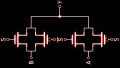
If you’re a pass-transistor partisan and find this somewhat disappointing, don’t worry. There’s yet another version of the SR gated latch:

This is absolutely a PTL configuration, because M1 and M2 are standard NMOS switches that pass inputs to outputs (and to the inputs of the inverters, which are also the outputs...). This circuit is widely used as the basic storage cell in static random access memory (SRAM); note that it requires only six transistors instead of eight. A thorough analysis of this circuit is not a straightforward task and is beyond the scope of this article.
Conclusion
Pass-transistor techniques are useful in a variety of digital design tasks, and we’ve seen that PTL plays a particularly prominent role in memory applications. We’ll conclude this series with the next article, which explores the issue of signal restoration in PTL circuits.