 Facebook
 Google
 GitHub
 Linkedin
How Should Data Converters Be Modeled for System Simulations?
This article launches a series exploring the question of how to model data converters for system simulations.
Engineers often wonder. Whilst working on various projects with tight design schedules, they often wonder about questions which they would like to find the answers to, but don’t have the time to. They still wonder.
In the course of his engineering work, your author has wondered about various questions concerning the transfer of data to and from an RF analog signal and I and Q digital signals. Recently, he has had time to pursue the answers to some of these questions, and has made whatever results he has been able to obtain available in technical articles. One such previous article addressed the question of “Should I and Q Combining and Separation Be Done Digitally or Analogly?” and another offered "Requirements for Good Communications Link Performance".
Figure 1 from that initial article shows the option of direct RF digital-to-analog conversion and direct RF analog-to-digital conversion. (Note that digital-to-analog converters {DACs} and analog-to-digital converters {ADCs} are jointly called “data converters”.)

Figure 1(a). Modulator

Figure 1(b). Demodulator
In that article, one thing your author wondered about was: what are the quality requirements for the DAC and ADC in Figure 1 for good communications link performance? There did not seem to be much published on this question.
This got him to wondering about, if he were to simulate a data converter in a communications link, how should it be modeled?
For bit error rate (BER) simulations, the number of bit errors found is divided by the total number of bits to calculate BER. For statistically significant results, there should be several hundred to a thousand errors counted. Even for a fairly high BER of 10-4; to count 500 errors takes 5 million bits. In order for the simulation to run in a reasonable short time, a fairly simple model, which captures adequately all the relevant data converter characteristics, must be found.
This article describes the information he found. It was useful to split the discussion into ones about ADCs and DACs. Note added in Version .02; Sigma-Delta type Data Converters are not considered in this article.
Models for Analog-to-Digital Converters (ADCs)
References [4] to [18] below discuss analysis, models, simulation, testing, and specifications for ADCs. In particular [13], [14], [16], and [17] present models which model some aspect of ADC performance. As an engineer, your author wondered if a simpler, easier to understand model was possible.
Figure 2 shows the quantization of a 5-bit ADC. There are 25 = 32 levels. Since the input can be positive and negative, this is called bi-polar input ADC. One aspect of this that your author had wondered about was the difference between dB relative to full scale (FS) between the peak and the average signal.
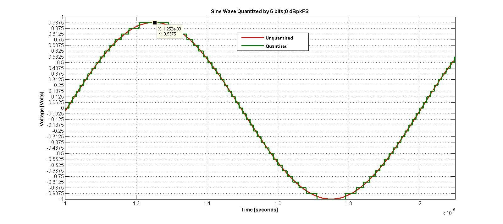
Figure 2.
The peak voltage of the signal in Figure 2 goes between +0.9375 Volt (FS+) and -1 Volt (FS-); which is ±1 Volt to a good approximation.
RF engineers are used to dealing with the rms values of signal. The rms value of the sine wave is 0.707 Volts, - 3 dB relative to FS. Since this has confused your author in the past, he has chosen to define the units dBpeakFS (dB of the voltage peak of the signal relative full scale), and dBrmsFS (dB of the rms value of the signal relative to full scale).
Another issue concerns the bandwidth of the ADC output that someone is concerned about. For early audio applications of ADCs, generally, folks were concerned about the full Nyquist bandwidth.
However, for direct RF sampling such as shown in Figure 1(b), only the portion of the Nyquist band occupied by the signal, plus a little for guard bands, is of concern. This led your author to define the “interesting bandwidth” as shown in Figure 3.
“Interesting bandwidth” is the bandwidth which is processed by the digital signal processing (DSP). It is usually the desired signal bandwidth or a little wider.

Figure 3.
Notice, in Figure 3, that although the signal and “interesting” bandwidths are shown to be the same, the center frequencies of the two are not. This can be due the bandpass sampling described in our first article, where the ADC clock acts as the local oscillator of a mixer. The frequency of the ADC clock will be denoted fS. The Nyquist frequency = FNyquist = fS/2.
Choice of an Input Signal for Implementing a Model
In order to characterize the ADC to create a good model, it is necessary to define a useful input signal. Most ADC specifications are created with a single sine wave input. However, since this has 0 Hz bandwidth and no envelope variation, it did not seem like a very good signal. A 2-tone input, shown in Figure 4, has more than 0 Hz bandwidth and has amplitude variation. It is easy to generate on the test bench using two high-quality signal sources and the correct power combining. In addition, most data sheets have some information on the device performance with a 2-tone input.
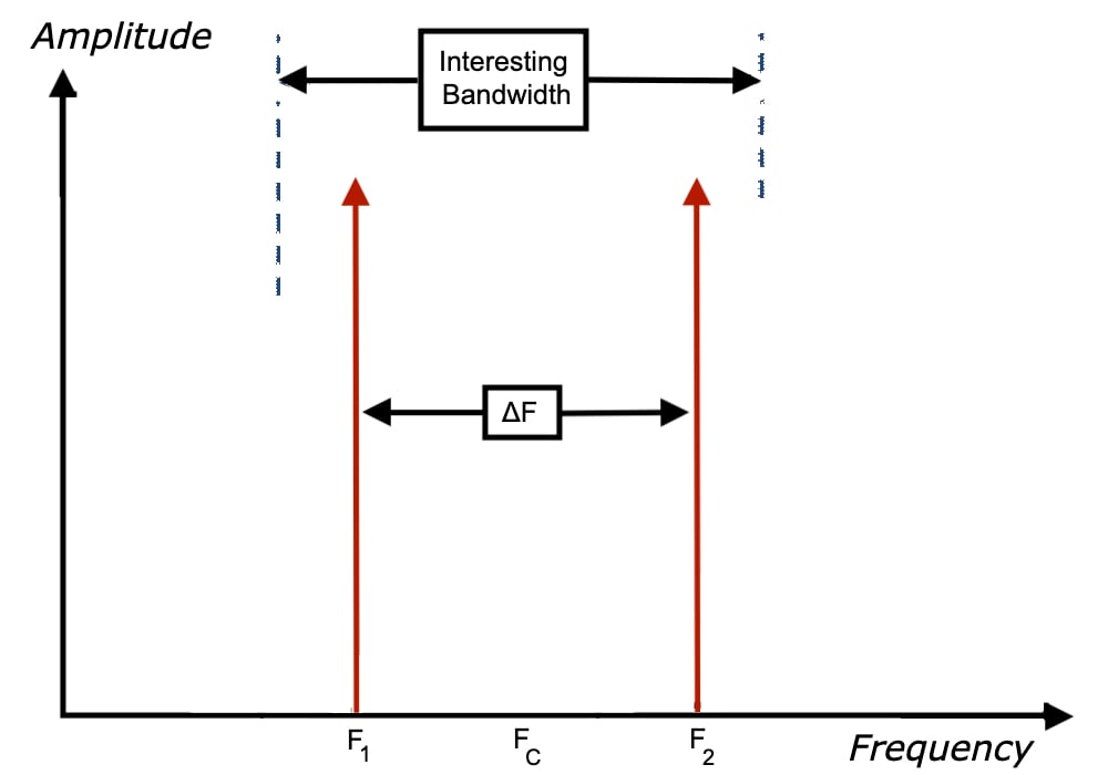
Figure 4.
A two-tone test signal was also proposed in [4] and [12]. Other test signals which have been proposed include a Gaussian input with an arbitrary spectrum shape [17] and AM or FM signals [5]. Typically, these require less common signal generators, and are not usually shown in datasheets as inputs for tests.
In the next article, we'll discuss an ADC model using an effective number of bits (ENOB).
For the rest of this series, please refer to the following table of abbreviations, glossaries, and references.
Abbreviations Used

Glossaries
Munson, Justin; "Understanding High Speed DAC Testing and Evaluation"; Analog Devices Application Note AN-928; 2013
Arrants, Alex; Brannon, Brad; & Reeder, Rob; "Understanding High Speed ADC Testing and Evaluation''; Analog Devices Application Note AN-835; 2010
Baker, Bonnie; "A Glossary of Analog-to-Digital Specifications and Performance Characteristics"; Texas Instruments Application Report SBAA147B; 2011
Malobert, Franco; Data Converters; Springer Publishing; Chapters 2: “Data Converter Specifications”; and 9: “Testing of D/A and A/D Converters”
Myderrizi, I; Zeki, A, "Current-Steering Digital-to-Analog Converters: Functional Specifications, Design Basics, and Behavioral Modeling," Antennas and Propagation Magazine, IEEE, vol.52, no.4, pp.197,208, Aug. 2010; Section 3. "Functional Specifications for Performance Characterization of a DAC"
References
General Information
[1] Brodsky, Wesley; “Should I and Q Combining and Separation be done Digitally or Analogly?”; WesBrodsky Wireless Communication White Paper: WBWC.01; 2014
[2] Maloberti, Franco; Data Converters; Springer Publishing; 2007
[3] VanTrees, Harry L; Detection, Estimation, and Modulation Theory, Part III, Radar/Sonar Signal Processing and Gaussian Signals in Noise; John Wiley and Sons; 1971. Appendix: “Complex Representation of Bandpass Signals, Systems, and Processes”
ADC Analysis, Models, Simulation, Testing, and Specifications
[4] Seokjin Kim; Elkis, R.; Peckerar, Martin, "Device Verification Testing of High-Speed Analog-to-Digital Converters in Satellite Communication Systems," Instrumentation and Measurement, IEEE Transactions on , vol.58, no.2, pp.270,280, Feb. 2009
[5] Vedral, J.; Fexa, P.; Svatos, J., "Using of AM and FM signal for ADC testing," Instrumentation and Measurement Technology Conference (I2MTC), 2010 IEEE , vol., no., pp.508,511, 3-6 May 2010
[6] Kester, Walt; "The Good, the Bad, and the Ugly Aspects of ADC Input Noise—Is No Noise Good Noise?"; Analog Devices Tutorial MT-004; 2008
[7] Arrants, Alex ; Brannon, Brad; Reeder, Rob; "Understanding High Speed ADC Testing and Evaluation"; Analog Devices Application Note AN-835; 2010
[8] Kester, Walt; "Understand SINAD, ENOB, SNR, THD, THD + N, and SFDR so You Don't Get Lost in the Noise Floor"; Analog Devices Tutorial MT-003; 2008
[9] Shinagawa, M.; Akazawa, Yukio; Wakimoto, Tsutomu, "Jitter analysis of high-speed sampling systems," Solid-State Circuits, IEEE Journal of , vol.25, no.1, pp.220,224, Feb 1990
[10] Hummels, D.M.; Irons, F.H.; Cook, R.; Papantonopoulos, I, "Characterization of ADCs using a non-iterative procedure," Circuits and Systems, 1994. ISCAS '94., 1994 IEEE International Symposium on , vol.2, no., pp.5,8 vol.2, 30 May-2 Jun 1994
[11] de Mateo Garcia, J.C.; Armada, AG., "Effects of bandpass sigma-delta modulation on OFDM signals," Consumer Electronics, IEEE Transactions on , vol.45, no.2, pp.318,326, May 1999
[12] Abuelma'atti, Muhammad Taher, "Effect of Nonmonotonicity on the Intermodulation Performance of A/D Converters," Communications, IEEE Transactions on, vol.33, no.8, pp.839,843, Aug 1985
[13] Traverso, P.A; Mirri, D.; Pasini, G.; Filicori, F., "A nonlinear dynamic S/H-ADC device model based on a modified Volterra series: identification procedure and commercial CAD tool implementation," Instrumentation and Measurement, IEEE Transactions on , vol.52, no.4, pp.1129,1135, Aug. 2003
[14] Fraz, H.; Bjorsell, N.; Kenney, J.S.; Sperlich, R., "Prediction of Harmonic Distortion in ADCs using dynamic Integral Non-Linearity model," Behavioral Modeling and Simulation Workshop, 2009. BMAS 2009. IEEE, pp.102,107, 17-18 Sept. 2009
[15] Kester, Walt; "ADC Noise Figure—An Often Misunderstood and Misinterpreted Specification"; Analog Devices Tutorial MT-006 ; 2014
[16] Brannon, Brad; MacLeod, Tom; "How ADIsimADC Models an ADC"; Analog Devices Application Note AN-737; 2009
[17] Dardari, D., "Joint clip and quantization effects characterization in OFDM receivers," Circuits and Systems I: Regular Papers, IEEE Transactions on, vol.53, no.8, pp.1741,1748, Aug. 2006
[18] Lavrador, Pedro Miguel; de Carvalho, N.B.; Pedro, Jose Carlos, "Evaluation of signal-to-noise and distortion ratio degradation in nonlinear systems," Microwave Theory and Techniques, IEEE Transactions on, vol.52, no.3, pp.813,822, March 2004
[18A] Gray, Robert M.; “Quantization Noise Spectra”; Information Theory, IEEE Transactions on; Vol. 36, No. 6; Nov. 1990; pages 1220 to 1244.
DAC Analysis, Models, Simulation, Testing, and Specifications
[19] Wikner, J.J.; Nianxiang Tan, "Modeling of CMOS digital-to-analog converters for telecommunication," Circuits and Systems II: Analog and Digital Signal Processing, IEEE Transactions on , vol.46, no.5, pp.489,499, May 1999
[20] Angrisani, L.; D'Arco, M., "Modeling Timing Jitter Effects in Digital-to-Analog Converters," Instrumentation and Measurement, IEEE Transactions on, vol.58, no.2, pp.330,336, Feb. 2009
[21] D'Apuzzo, M.; D'Arco, M.; Liccardo, A; Vadursi, M., "Modeling DAC Output Waveforms," Instrumentation and Measurement, IEEE Transactions on, vol.59, no.11, pp.2854,2862, Nov. 2010
[22] Myderrizi, I; Zeki, A, "Current-Steering Digital-to-Analog Converters: Functional Specifications, Design Basics, and Behavioral Modeling," Antennas and Propagation Magazine, IEEE, vol.52, no.4, pp.197,208, Aug. 2010
[23] Sang Min Lee; Taleie, S.M.; Saripalli, G.R.; Dongwon Seo, "Clock-Phase-Noise-Induced TX Leakage Estimation of a Baseband Wireless Transmitter DAC," Circuits and Systems II: Express Briefs, IEEE Transactions on , vol.59, no.5, pp.277,281, May 2012
[24] Naoues, M.; Morche, D.; Dehos, C.; Barrak, R.; Ghazel, A, "Novel behavioral DAC modeling technique for WirelessHD system specification," Electronics, Circuits, and Systems, 2009. ICECS 2009. 16th IEEE International Conference on, vol., no., pp.543,546, 13-16 Dec. 2009
[25] Kitaek Bae; Changyong Shin; Powers, E.J., "Performance Analysis of OFDM Systems with Selected Mapping in the Presence of Nonlinearity," Wireless Communications, IEEE Transactions on , vol.12, no.5, pp.2314,2322, May 2013
[26] Ling, W.A, "Shaping Quantization Noise and Clipping Distortion in Direct-Detection Discrete Multitone," Lightwave Technology, Journal of, vol.32, no.9, pp.1750,1758, May1, 2014
[27] Engel, G.; Fague, D.E.; Toledano, A, "RF digital-to-analog converters enable direct synthesis of communications signals," Communications Magazine, IEEE, vol.50, no.10, pp.108,116, October 2012
[28] Pearson, Chris; "High Speed, Digital to Analog Converters Basics"; Texas Instruments Application Report SLAA523A; 2012
[29] Munson, Justin; "Understanding High Speed DAC Testing and Evaluation"; Analog Devices Application Note AN-928; 2013


In paragraph 6, the exponential notation did not come out right. The corrected paragraph, with direct numerical notation, is below:
“For bit error rate (BER) simulations, the number of bit errors found is divided by the total number of bits to calculate BER. For statistically significant results, there should be several hundred to a thousand errors counted. Even for a fairly high BER of 0.0001 to count 500 errors takes 5 million bits. In order for the simulation to run in a reasonable short time, a fairly simple model, which captures adequately all the relevant data converter characteristics, must be found.”
Also, in the paragraph immediately before the title “Choice of an Input Signal for Implementing a Model” and in the Table “Abbreviations Used”; “fS” should be f(subscript)S; denoting sampling frequency.