Facebook
 Google
 GitHub
 Linkedin
How to Design a Schematic: Creating a Roadmap for a Custom PCB Inclinometer
This project series details the design and construction of a precision inclinometer based on the Murata SCA103T-D04. This article looks at schematic design considerations.
How do you create a schematic for a custom PCB? This article will discuss the steps of designing a schematic for a board using the example of an inclinometer subsystem.
I recently designed a custom PCB for an inclinometer subsystem. In this article, we'll go into how to design a functional schematic, the first step in any successful project.
In most designs, parts are chosen based on requirements of availability, cost, reliability, etc. It's important to note, however, that AAC projects are designed to be educational and impartial in nature, so your part selection and design may vary based on your needs and preferences.
Let's go through this large schematic section by section, starting with power.
Power
The project is supplied with 9-12V DC power from a DC barrel jack connected to a wall-wart power supply. If the wall-wart supply is too noisy, I can replace it with a lab-grade power supply or battery pack. A low profile 3.5mm DC barrel jack was selected for the design because it is the approximate height of other tall components on the board.
There are three Texas Instrument TPS709xx LDOs that supply 2.5V, 3.3V, and 5.0V digital rails, while the LT1027LS8 is the voltage reference chip used to provide the 5V analog rail.
Voltage references do not typically directly power ICs without support circuitry. However, the demands on this IC are well within its current sourcing capabilities with a safety factor of 2-3. It will support the SCA103T-DO4 (5 mA max consumption) and the IRef of the LTC2380-24 (2.1 mA max) and is capable of sourcing 15 mA. The maximum values were provided in the datasheet and the typical values are slightly less than the numbers listed above.
The LT1027 has a noise reduction pin that can be tied to a mylar capacitor. This capacitor will significantly reduce the wideband noise of the LT1027LS8 in a 10Hz to 1kHz bandwidth. The capacitor has a guard ring whose voltage is determined by a resistor-divider circuit. Capacitors are added to input and outputs as suggested in the relevant datasheets.

The power portion of the schematic. Click to enlarge.
As a note, now that I've completed this board, I have the benefit of hindsight. If I were to make another spin of this circuit, I would likely choose a different VREF design that includes a buffer between VREF and the inclinometer/ADC.
USB-to-UART Converter
The CP2102N USB-to-UART converter used in this schematic is the same circuit I have used in past designs. (You can find more information in these articles: Building a Capacitive Touch Interface with the Texas Instruments MSP430, Tales of Project Troubleshooting.)
Remember when programming the CP2102N for the first time from a Windows-based machine to use a USB2.0 port. Windows does not properly enumerate the device from a USB3.0 port.
D2 provides ESD protection for the USB board input, and D3 provides an indication that UART data is indeed moving between the CP2102N and the MSP430. The CP2101N GPIO0 and GPIO1 outputs have to be adjusted to their “Alternate Function” in Simplicity Studio to enable the D3 indicator LEDs. Decoupling capacitors and a resistor-divider are provided per datasheet recommendations.
This is the IC that started the whole project. muRata’s Ville Nurmiainen graciously supplied the SCA103T for this project. Click to enlarge.
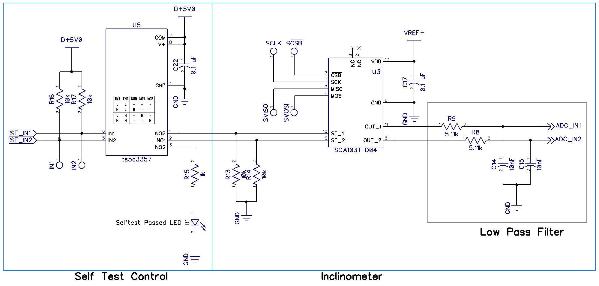
The muRata SCA103T-D04 has a built-in 11-bit ADC that I did not use. Still, it might be interesting to experiment with, so I included four test pads for possible future use.
The IC has two self-test pins that control the self-test functionality of the two different internal sensors. These self-test pins are connected to the two separate sensing channels in the SCA103T-D04. When activated, the IC generates an electrostatic force that deflects the proof mass inside each sensing element. The force displaces the mass to its upper limit, and the output of that channel approaches its maximum value. The datasheet indicates that both self-test pins should not be activated at the same time, so I incorporated the TI TS5A3357 SP3T IC to actively prevent it. The logic diagram of this switch is shown below.

Logic diagram of the TS5A3357 switch. Image from the datasheet
This IC provides three normally-open outputs that connect to a common line, so the plan is to use two GPIO pins from the MSP430 to control the TS5A3357. The TSA5A3357, in turn, controls the self-test functionality of the SCA103T, as well as a status indicator LED that can programmatically be used to indicate a pass or fail condition, perhaps with a solid or blinking LED.
The inclinometer has two acceleration sensors arranged in a line, but pointing in opposite directions that provide differential output. Following the datasheet recommendation, a single-pole RC filter (fc=3.1kHz) is used “to minimize clock noise” on each output.
Signal Buffer and Analog-to-Digital Converter

The signal buffer and low-pass filter
After the signals from the inclinometer pass through the low pass filter, they enter the AD8244 signal buffer. This unity-gain quad op-amp isolates the SCA103T outputs from the LTC2380 inputs.
Successive approximation registers can disturb the signal they are attempting to quantize. Adding this device allows the inclinometer to provide an analog signal to the high-impedance side of the buffer. The low-impedance output buffer is more than capable of delivering that same signal voltage to the SAR ADC regardless of current demands.
An additional filter is included between the buffer and the ADC per datasheet recommendation.
MSP430FR2633

Schematic of the MSP430 portion of the design
I have used the MSP430FR2633 IC on the past several projects and plan to continue including something in the product family on future projects while I learn more about programming in Code Composer Studio.
There are several capacitive-capable touch-pins available as well as multiple GPIOs. The SPI output of the ADC feeds into the MSP430 and the SPI output of the MCU feeds the off-board connector since the ADC does not have an SPI MOSI pin. Future functionality might include a display of some kind.
S1 is used during programming to select the voltage reference for the MCU (programmer or board). S2 switch decoupling resistor values are recommended by Texas Instruments in the MSP430 datasheet.
Firmware Programming
The firmware for the device will be covered in a future article, but the schematic design determines which pins are attached to which nets, and now is as good a time as any to incorporate the design choices into the firmware. The MSP430 uses memory registers to control pins. So each pin corresponds to a bit in a register that I will interact with later.
#define UART_RX_PIN     BIT5            // P2.5 eUSCI_A1
#define UART_TX_PIN     BIT6            // P2.6 eUSCI_A1

#define SPI_EN_PIN      BIT0            // P1.0 eUSCI_B0 -- not used
#define SPI_CLK_PIN     BIT1            // P1.1 eUSCI_B0
#define SPI_MOSI_PIN    BIT2            // P1.2 eUSCI_B0 -- not used yet
#define SPI_MISO_PIN    BIT3            // P1.3 eUSCI_B0

#define ADC24_RDL       BIT0            // P3.0 set low always
#define ADC24_CNV       BIT1            // P3.1 L->H->L (20 ns) to convert
#define ADC24_BUSY      BIT4            // P2.4 goes low after conversion

#define ST_IN1          BIT0            // 3PST switch input 0
#define ST_IN2          BIT1            // 3PST switch input 1
Downloadable Schematic
This article is meant to serve as supplemental information for my larger project, but it can also provide insights into how to create a schematic for a custom board project.
What else would you like to know about schematic creation? If you have any questions or insights, please share them in the comments below.
You can download the full schematic below.
Next, read how I turned this schematic into a PCB layout.
Related Content