 Facebook
 Google
 GitHub
 Linkedin
How to Write the VHDL Description of a Simple Algorithm: The Control Path
This article will review converting a simple algorithm into a VHDL description.
Steve Arar continues his VHDL series with this discussion on converting a simple algorithm into a VHDL description—this time focusing on the control path portion of a digital design.
In my last article, I described how to write the VHDL description of a simple algorithm. I laid out the difference between the data path and the control path in digital design and then proceeded to dive into the data path. In this article, we'll instead take a look at the control path.
This article will review converting a simple algorithm into a VHDL description. We will use a least common multiple (LCM) algorithm as an example.
Review of the Data Path
In the previous article, we saw that to implement the data path of the LCM algorithm described by the pseudocode in Listing 1, we can use the schematic shown in Figure 1.
Listing 1
1	a=m
2	b=n
3	while (a != b)
4	{
5		if ( a < b )
6		{
7			a=a+m
8			b=b
9		}
10		else
11		{
12			a=a
13			b=b+n
14		}
15	}
16	lcm=a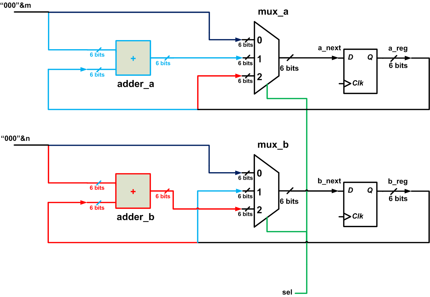
Figure 1
By applying the appropriate logic levels to the select input of the multiplexers, we can select which operation will be performed. In this article, we’ll design the circuit that generates an appropriate “sel” signal so that the data path of Figure 1 performs the operations needed to calculate the LCM of the inputs.
Modifying the Pseudocode to Fit the Description of an FSM
In Figure 1, the “sel” signal must have three different values so that it can choose one of the three inputs to the multiplexer. Thus, it is reasonable to expect that we will need a three-state FSM, where each state corresponds to one of the three inputs, but we will see that the FSM can actually be implemented with only two states.
The next state of the FSM will be chosen based on the flow of the algorithm in Listing 1. The flow of the algorithm refers to either going to the next line or jumping to a particular point in the code, according to the “while” and “if” structures. To make the pseudocode of Listing 1 closer to an FSM description, let’s rewrite the “while” statement as follows:
Listing 2
1	a=m
2	b=n
3	if (a=b)
4	{
5		goto line 28
6	}
7	else
8	{
9		if ( a < b )
10		{
11			a=a+m
12			b=b
13		}
14		else
15		{
16			a=a
17			b=b+n
18		}
19	}
20	if( a=b )
21	{
22		goto line 28
23	}
24	else
25	{
26		goto line 9
27	}
28	lcm=a
This new version uses “if-else” structures to replace the “while” statement; this makes it easier to design the FSM for the algorithm. The conditions of these “if” statements can actually give us some hints about the conditions for the FSM transitions from one state to another.
To make the above algorithm more practical, we will add some other features: we’ll assume that the LCM circuit has a “ready” output and a “start” input. When the “ready” output is logic high, we know that the system is in the "idle" mode and is ready to work on a new pair of input values. Also, asserting the “ready” output high means that the circuit has finished finding the LCM of the previous inputs. Hence, when we reach the end of the algorithm, we should set the “ready” output to logic high.
Moreover, when a valid pair of input values is applied to the LCM circuit, we set the “start” input to logic high to let the circuit know that it should start the algorithm.
The ASMD Chart of an Algorithm
To find the VHDL description of an algorithm, we can draw different states of the control path in a chart called an ASMD, which stands for Algorithmic State Machine with a Data path. The ASMD chart not only represents the FSM of the control path but also describes the register transfer operations of the data path. We will use the LCM algorithm as an example of how to derive the ASMD chart of a given algorithm.
Based on our discussion so far, it seems that we should use a three-state FSM. Each state of the FSM can update the value of the a and b registers, assign some values to the circuit outputs such as the “ready” output, and check the conditions of the “if” structures to determine the next state of the FSM. All of these pieces of information can be represented by the ASMD chart of the algorithm.
Let’s proceed with the LCM algorithm: We will call the initial state of the system “idle”. In this state, the system is ready to accept new input pairs, so “ready” is set to high. As shown in Figure 2, we can use a rectangle to represent this state. The name of the state (i.e., “idle”) is written above the rectangle, and the assignment corresponding to the “ready” output is written inside the rectangle.
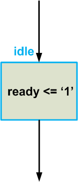
Figure 3
What other parts of the algorithm can be performed in this state? If the “start” input is logic low, we shouldn’t start the calculations, probably because the inputs are not valid yet. Hence, for “start”=‘0’, we should remain in the “idle” state. However, when “start” is logic high, we should store the inputs, m and n, in the a and b registers, respectively, and start the calculations. We can perform storing m and n in the "idle" state.
To represent conditional structures, we will use a green hexagon shape. For the conditional assignments of the algorithm, we’ll use a red ellipse. From that, we obtain:
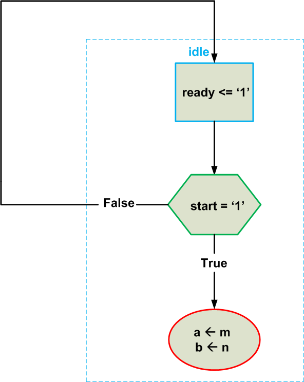
Figure 4
Note that the assignments to registers are shown by an arrow , e.g., a ← m. This notation is used to emphasize that such assignments will take effect at the next clock edge. However, the assignment corresponding to the “ready” output is represented by “<=” notation. This means that when we are in the “idle” state, the “ready” output is always logic high, regardless of the state of the clock. Also note the dashed box in Figure 4, which indicates that all of these operations are performed in the “idle” state.
Next, we reach the “if” statement of Line 3, which compares a and b in order to determine the next operation. When a=b, the algorithm is finished and we can assign the value of a to the output lcm; this can be done in a new state. However, there’s another alternative: we can unconditionally assign the value of a to lcm but consider the value of lcm valid only when the algorithm is finished.
In other words, lcm is valid only when the “ready” output is high. Hence, we can simply check the condition a=b to decide if the algorithm is finished (in which case we return to the “idle” state) or if we have to proceed with the rest of the algorithm. So far we have the following chart:
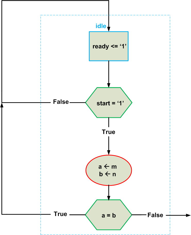
Figure 5
Keep in mind that, though not shown in Figure 5, the output lcm is equal to a and is valid when “ready” is logic high.
Now, let’s examine the “if” statement of Line 9. Can we check the condition $$a \leq b$$ in the “idle” state? Note that the “if” structure beginning at Line 9 constitutes the main calculations of the LCM algorithm, and because of the “if” statement at Line 20, we may loop back to the Line 9 “if” statement several times. That’s why I suggest placing the Line 9 “if” statement in a new FSM state. It should be noted that we could create several ASMD charts for a given design, but some of these ASMDs may need more states or more conditional blocks.
After adding the required blocks for the next state of the ASMD chart, we arrive at the complete chart of the algorithm, shown in Figure 6. As you can see, the next state is named “op”. The first conditional block of this state compares a with b and performs the required operation according to the result of the comparison. Finally, the condition $$a=b$$ is checked. If this condition is evaluated as true, the algorithm ends and the system goes to the “idle” state. Otherwise, it returns to the “op” state, as specified by Line 26 of the pseudocode.
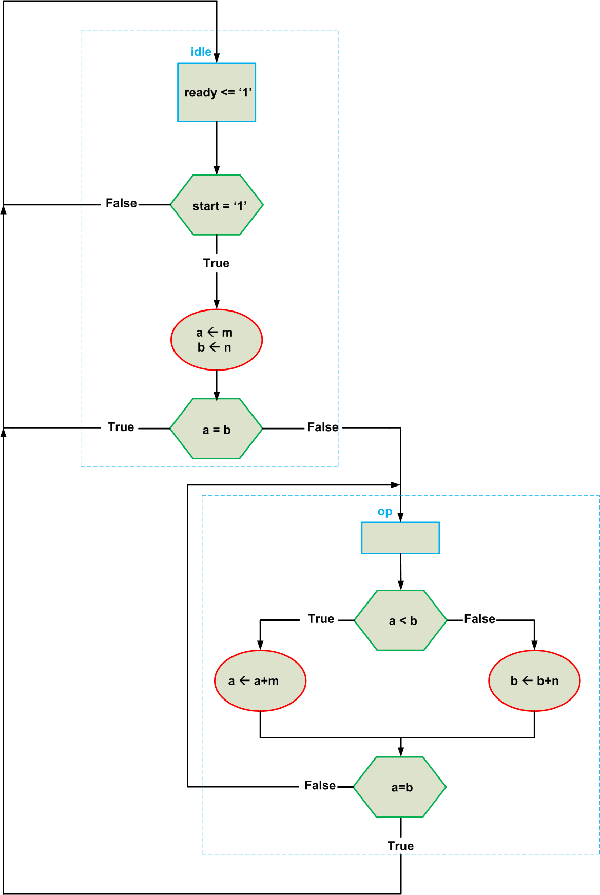
Figure 6
There are a few points that need further attention: First, the ASMD chart only shows the registers whose value has changed. For example, Lines 12 and 16 of Listing 2 are not shown in Figure 6. Moreover, as you see, the output “ready” is logic high in the “idle” state but its value is not given for the “op” state. This is the way we specify that the “ready” output is high only in the “idle” state and, hence, it would be considered logic low in the “op” state.
Second, be careful about conditional blocks that are placed after an assignment to the register. Note that the assignment to the register will take effect at the next clock tick. That’s why we should be careful when using the value of a register in conditional blocks: should we use the current value of the register or its next value? The ASMD chart that we have created is based on pseudocode in which the value of a variable gets updated right after a given assignment. This means that we should use the next value of the a and b registers in our chart.
We’ll define two new signals add_a and add_b equal to a+m and b+n, respectively, and then we can redraw the chart of Figure 6 as shown in Figure 7. Note that the conditional blocks now use the next value of the registers in comparisons.
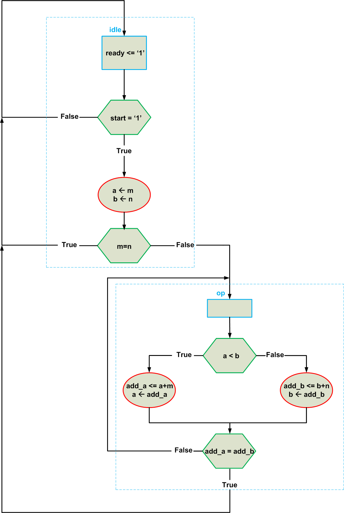
Figure 7
Third, while we were originally planning to design a three-state FSM, the chart in Figure 7 shows that our FSM has only two states. As you can see, two sets of assignments to the a and b registers (Lines 11-12 and Lines 16-17 of Listing 2) are placed inside a single state, namely, the “op” state; however, there will be no conflict between these two sets of assignments because only one of them can be executed in a given clock cycle.
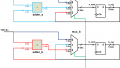
In fact, for the flowchart of Figure 7, the multiplexers of the data path will be implemented as shown in Figure 8. The value of the sel signal, which represents the state of the FSM, is either one or zero. However, when the FSM is in the “op” state, the output of a comparator block will determine whether Lines 11 and 12 of the pseudocode should be executed or Lines 16 and 17.
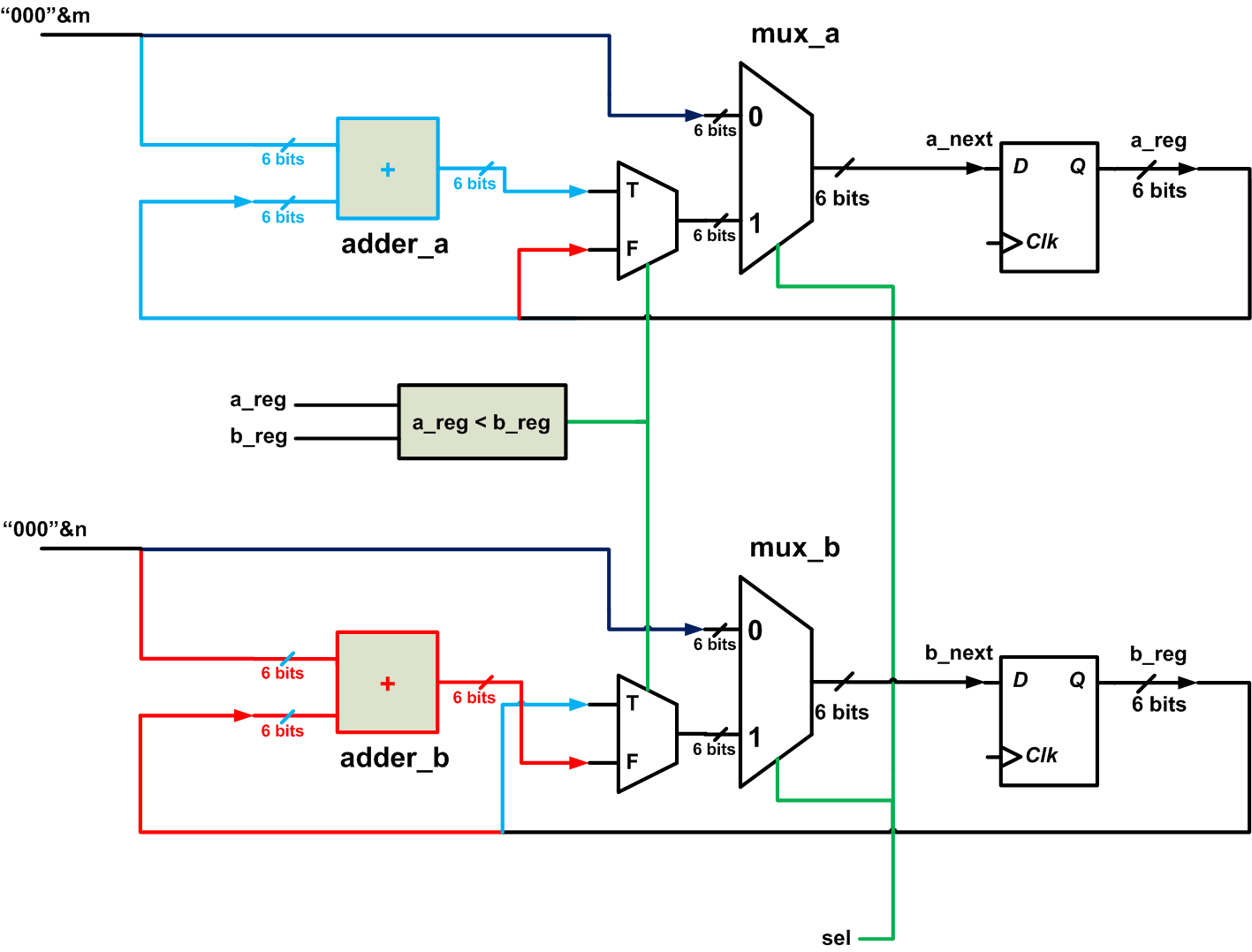
Figure 8
Based on the ASMD chart of Figure 7 and the schematic of Figure 8, we can find the VHDL description of the algorithm, which is given in Listing 3 below. The comments in the VHDL code give some hints about the hardware that each code segment is referring to.
Listing 3
1	library IEEE;
2	use IEEE.STD_LOGIC_1164.ALL;
3	use IEEE.NUMERIC_STD.ALL;

4	entity lcm_fsmd is

5		port( clk, reset: in std_logic;
6		           start: in std_logic;
7		           m, n: in std_logic_vector(2 downto 0);
8		           ready: out std_logic;
9		           lcm: out std_logic_vector(5 downto 0));

10	end lcm_fsmd;

11	architecture lcm_arch of lcm_fsmd is

12		type state_type is (idle, op);
13		signal state_reg, state_next: state_type;
14		signal a_reg, a_next, b_reg, b_next: unsigned(5 downto 0);
15		signal add_a, add_b: unsigned(5 downto 0);

16	begin

17		--control path: registers of the FSM
18		process(clk, reset)
19		begin
20			if (reset='1') then
21				state_reg <= idle;
22			elsif (clk'event and clk='1') then
23				state_reg <= state_next;
24			end if;
25		end process;

26		--control path: the logic that determines the next state of the FSM (this part of
--the code is written based on the green hexagons of Figure 7)
27		process(state_reg, start, m, n, add_a, add_b)
28		begin
29			case state_reg is
30				when idle =>
31					if ( start='1' ) then
32						if ( m=n ) then
33							state_next <= idle;
34						else
35							state_next <= op;
36						end if;
37					else
38						state_next <= idle;
39					end if;

40				when op =>
41					if ( add_a = add_b ) then
42						state_next <= idle;
43					else
44						state_next <= op;
45					end if;

46			end case;
47		end process;

48		--control path: output logic
49		ready <= '1' when state_reg = idle else
50					'0';

51		--data path: the registers used in the data path
52		process(clk, reset)
53		begin
54			if ( reset='1' ) then
55				a_reg <= (others => '0');
56				b_reg <= (others => '0');
57			elsif ( clk'event and clk='1' ) then
58				a_reg <= a_next;
59				b_reg <= b_next;
60			end if;
61		end process;

62		--data path: the multiplexers of Figure 8
63		process(state_reg, m, n, a_reg, b_reg, add_a, add_b)
64		begin
65			case state_reg is
66				when idle =>
67					a_next <= unsigned( "000" & m);
68					b_next <= unsigned( "000" & n);

69				when op =>
70					if ( a_reg < b_reg ) then
71						a_next <= add_a;
72						b_next <= b_reg;
73					else
74						a_next <= a_reg;
75						b_next <= add_b;
76					end if;

77			end case;
78		end process;

79		--data path: functional units
80		add_a <= unsigned(("000" & m)) + a_reg;
81		add_b <= unsigned(("000" & n)) + b_reg;

82		--data path: output
83		lcm <= std_logic_vector(a_reg);

84	end lcm_arch;
Figure 9 shows an ISE simulation for the above code.
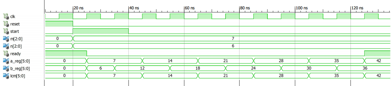
Figure 9
For this simulation, the inputs are m=7 and n=6. At the end of the algorithm, when the “ready” output goes to high, the lcm output is 42, which is the least common multiple of 7 and 6.
Summary
- An FSM can be used as the controller for the data path of an algorithm.
- By writing the algorithm using “if” statements, we can more easily design the FSM for the algorithm. The conditions of the “if” statements can actually give us some hints about the conditions for the FSM transitions from one state to another one.
- The ASMD chart not only represents the FSM of the control path but also describes the register transfer operations of the data path.
- It is possible to create multiple ASMD charts for a given design, but some of these ASMDs may need more states or more conditional blocks.
To see a complete list of my articles, please visit this page.


help me with the testbench