Facebook
 Google
 GitHub
 Linkedin
How to Write the VHDL Description of a Simple Algorithm: The Data Path
In this article, you'll learn how to write the VHDL code for a simple algorithm.
In this article, you'll learn how to write the VHDL code for a simple algorithm.
This article will review converting a simple algorithm, such as a least common multiple (LCM) algorithm, into a VHDL description. The data path of the algorithm will be discussed in this article. In the next article, we’ll discuss the control path of the algorithm.
Separating Data Path from Control Path
Traditional digital design splits a given problem into two sections: a data path and a control path (or a controller). As a familiar example, consider a microprocessor that consists of an arithmetic logic unit (ALU) and a control path. The ALU may have several arithmetic units, such as adders and multipliers. The data processing is performed by the ALU, and that’s why the ALU is considered as the data path of this system. The control path determines which operation will be performed by the ALU. By specifying a particular sequence of operations, the control unit can implement a given algorithm.
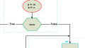
The following block diagram shows the idea of separating a system into a data path and a control path.
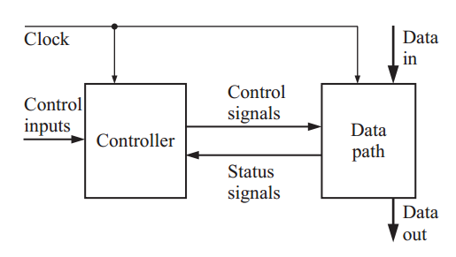
Figure 1. A controller and a data path work together to implement an algorithm. Image courtesy of Digital Systems Design Using VHDL.
As you can see in the diagram, some of the system inputs go to the controller and some go into the data path. For example, there may be a “start” input that will trigger a multiplication algorithm implemented by the system.
In this case, “start” corresponds to one of the “control inputs” shown in the diagram and the multiplication operands correspond to the “data in.” The controller also receives some inputs as “status signals” from the data path. A multiplication overflow flag is an example of a “status signal.” Based on the control inputs and the status signals, the controller determines the upcoming operations for the data path.
Separating the data path from the controller allows us to more easily find the errors in the design process. Moreover, this design methodology makes future modifications of the system easier.
To further explore this design method, we’ll use the example of a least common multiple (LCM) algorithm implemented as a VHDL description.
The Pseudocode of an LCM Algorithm
Listing 1 shows the pseudocode to find the LCM of m and n. Let’s assume that $$1 \leq m \leq 7$$ and $$1 \leq n \leq 7$$.
Listing 1
1	a=m
2	b=n
3	while (a != b)
4	{
5		if ( a < b )
6			{
7			a=a+m
8			}
9		else
10			{
11			b=b+n
12			}
13	}
14	lcm=a
This algorithm uses repeated addition operations to find the multiples of m and n. These multiples are stored in a and b, respectively. After each iteration of the algorithm, we check a and b; if they are equal, we have found a common multiple and the algorithm ends. Since the smaller multiples are checked first, the algorithm will give the LCM of m and n.
Find the Building Blocks of the Data Path
Let’s see what building blocks are required to implement the data path of the above algorithm in hardware. A computer programming language uses a “variable” to store information that will be referenced or used later. We can use some flip-flops as memory elements to store the value of the variables a and b. These two registers must be wide enough to store the LCM of m and n. Since $$1 \leq m \leq 7$$ and $$1 \leq n \leq 7$$, the LCM will be smaller than $$7 \times 6=42$$. (Note that the LCM of 7 and 7 is 7.) Hence, we need two six-bit registers to implement a and b.
Moreover, considering lines 7 and 11 of the code, we need two adders to calculate a+m and b+n. Since the maximum value of this addition result is 42, six-bit adders are wide enough to avoid addition overflow.
The code suggests that we also need some multiplexers. Why? Consider lines 1 and 7 of the code. In line 1, we are assigning the value of m to the register a. In line 7, we are assigning the result of the addition a+m to the register a. Hence, a multiplexer is required to choose one of these values and assign it to the register a. If we examine the code more closely, we’ll see that there’s one other possible assignment. To see this implied assignment, we can rewrite the code as follows:
Listing 2
1	a=m
2	b=n
3	while (a != b)
4	{
5		if ( a < b )
6			{
7			a=a+m
8			b=b
9			}
10		else
11			{
12			a=a
13			b=b+n
14			}
15	}
16	lcm=a
As you see, sometimes we are simply retaining the current value of a and b (lines 12 and 8, respectively). Since there are three different values that can be assigned to each of the a and b registers, we’ll need two three-to-one multiplexers. The required blocks are shown in Figure 2.
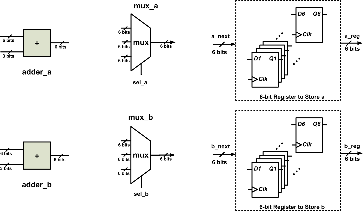
Figure 2
Connect the Components
The following figure shows a possible connection of these components for implementing the above algorithm. In this figure, the set of D-type flip-flops (DFFs) used to store the values of a and b are represented by a single DFF.
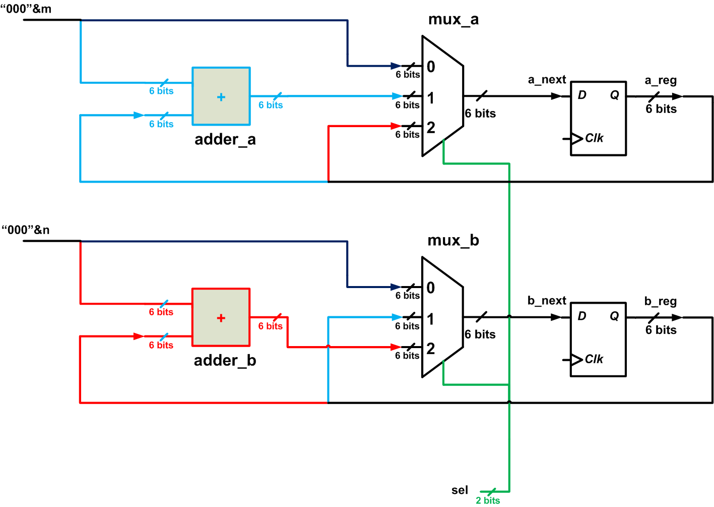
Figure 3
As you can see, the control input sel goes to the select input of the two multiplexers. By choosing different values for sel, we can perform the three assignments of the algorithm. For example, when the two multiplexers choose the input denoted by “0”, the inputs m and n will be passed to a_next and b_next, respectively. With the upcoming clock edge, the a and b registers will be updated with the value of the inputs m and n, respectively. This corresponds to Lines 1 and 2 of Listing 2. Note that we are assigning m and n, which are three-bit numbers, to a and b, which are six-bit registers. That’s why, in Figure 3, the concatenation operator is used to append three zeros to the left of m and n (and this in turn is why the adders in Figure 3 have two six-bit inputs, in contrast to the adders in Figure 2, which have a three-bit input and a six-bit input).
When the two multiplexers of Figure 3 select the input denoted by “1”, the next value of a will be equal to m plus the current value of the a register. In this case, the b register will retain its current value. This corresponds to lines 7 and 8 of Listing 2. Similarly, the multiplexers can choose the red paths, which will correspond to lines 12 and 13 of Listing 2.
The schematic of Figure 3 can perform the required operations on the inputs m and n; however, an appropriate signal must be generated for the select input of the multiplexers. At the beginning of the algorithm, sel will choose the path in dark blue to update the registers with the value of the inputs. For the rest of the algorithm, either the light blue paths or the red paths will be chosen. This choice will be made based on the result of the comparison of a and b ( see lines 5 and 10 of Listing 2). Hence, two other circuits need to be added to the schematic of Figure 3: a circuit to compare a with b, and one to generate an appropriate signal for the sel input. Comparing two binary numbers is a trivial task, but what about generating the sel signal? By determining which operations will be performed, the sel signal is actually specifying the state of the system, and thus it is not surprising that we can use a finite state machine (FSM) to generate sel. An FSM is in exactly one of a finite number of states at any given time, and it can be designed to go from one state to another in response to certain conditions. In the case of the LCM example, a state transition can occur in response to the result of the comparison between a and b.
We will discuss the control path of the LCM algorithm in the next article, and then we will use our findings to write the VHDL code for the algorithm.
Summary
- Traditional digital design splits a given problem into two sections: a data path and a control path (or a controller).
- The data path performs the actual processing on the input data, and the control path determines which operation should be performed by the data path.
- Separating the data path from the controller makes it easier to find design errors and implement modifications.
- An FSM can be used to generate the signal for the select input of the routing multiplexers in the data path.
To see a complete list of my articles, please visit this page.