 Facebook
 Google
 GitHub
 Linkedin
Introduction to Servo-Loop ADC Testing
Servo-loop testing allows the determination of an analog-to-digital converter (ADC) transfer function. This article will describe the basics of servo-loop ADC testing and illustrate several different servo-loop test configurations.
The static parameters of an A/D converter (ADC) provide an understanding of the device behavior for DC or slowly changing signals. However, to determine the static parameters— including offset and gain errors, differential nonlinearity (DNL), and integral nonlinearity (INL)—we first need to determine the DC transfer function of the ADC. Servo-loop testing is a classical industrial method for determining the ADC transfer function.
ADC vs. DAC Testing
Testing an ADC can be much more difficult than testing a D/A converter (DAC). This stems from the DAC transfer curve being a one-to-one mapping function, whereas the ADC characteristic curve is a many-to-one mapping function. This is illustrated in Figure 1.
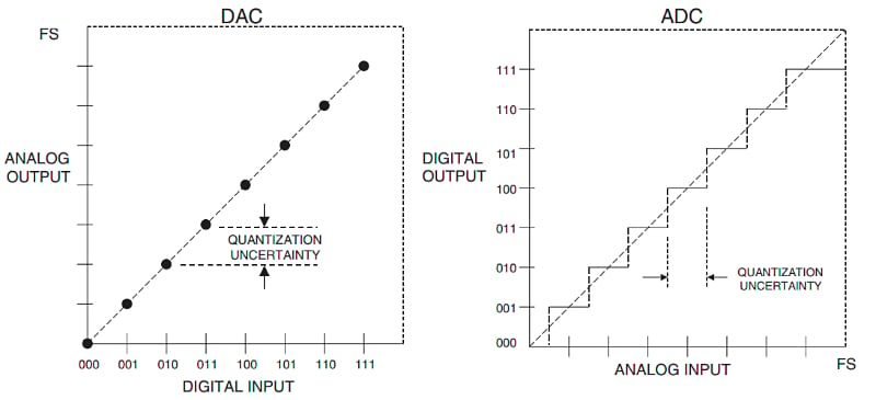
Figure 1. DAC and ADC transfer curves. Image used courtesy of Analog Devices.
Figure 1 shows the ideal characteristic curves of a 3-bit unipolar DAC and a 3-bit unipolar ADC. For the DAC, both the input and output are quantized, and the transfer function consists of eight points. Being a one-to-one mapping function, we can easily measure the DAC output voltage for each digital code and determine its transfer curve. On the other hand, a given ADC output code corresponds to a continuous range of input values. Therefore, we cannot determine the ADC transfer function by applying a known voltage to the ADC input and measuring the output code.
To fully determine the ADC transfer curve, we must measure its code transition points. This makes ADC testing complicated and expensive. In fact, about 15 to 20% of the unit selling price of an ADC is due to different testing procedures. Researchers in academia and industry have carried out a significant amount of research to find efficient ADC testing methods. One popular method is servo-loop testing which is discussed below.
Servo-loop ADC Testing
Servo-loop testing, first introduced in 1975, is a feedback-based technique to determine the ADC transition points. A basic configuration of the test setup is shown in Figure 2.
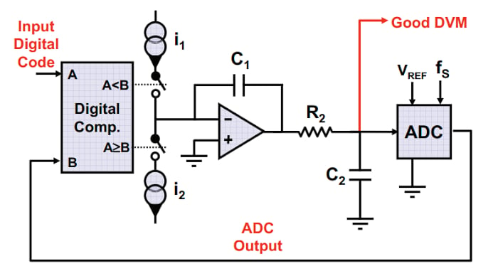
Figure 2. Basic servo-loop test configuration. Image used courtesy of H. Khorramabadi
The feedback loop consists of a digital comparator, two current sources (I1 and I2), an op-amp configured as an analog integrator, and the ADC under test. To determine a given transition point, the corresponding code is applied to the “A” input of the comparator. This value is compared with the ADC output code (the ADC output is connected to the other, "B", input of the comparator). If the ADC output is greater than the target code (B > A), the comparator turns on the upper switch for a specific time period Δt. With I1 flowing through C1, the integrator output decreases by:
$$\Delta V = \frac{I_1}{C_1}\Delta t$$
This consequently reduces the ADC output code and brings it closer to the target code applied to the “A” input of the comparator. This procedure continues until the ADC input is within one step (ΔV) from the target transition point. During the next cycle, the ADC input is reduced by another ΔV, making the ADC output less than or equal to A (B ≤ A). At this point, the comparator turns on the lower switch and increases the integrator output by:
$$\Delta V = \frac{I_2}{C_1}\Delta t$$
Normally, the two current sources have the same value; hence, the step size in either direction is the same. Since the ADC input is within one step from the transition point, the subsequent steps will make the ADC input cross the transition point on every cycle. In other words, the ADC will output a sequence of codes that are greater than A (B < A) or less than or equal to A (B ≤ A), alternately.
Transient Response and Oscillatory Behavior
Figure 3 should help you better visualize the system response. The figure shows how the ADC input voltage approaches the code transition point. The figure shows the waveform for two different simulations with different initial values. In one simulation, the initial value of the ADC input is 10 steps (10ΔV) larger than the target code transition point. In the second one, the initial value is 10.001 steps away from the code edge.
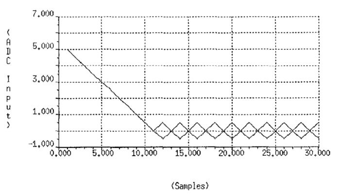
Figure 3. Transient response of servo-loop testing demonstrating oscillatory behavior. Image used courtesy of S. Max (subscription required)
A few observations are worth mentioning here. First, the ADC input is not actually equal to the transition voltage. The loop enters an oscillating state where the ADC input voltage is a triangular wave oscillating around the transition level (we are ignoring the filtering effect that R2 and C2 might introduce). The average value of the triangular waveform provides an estimate of the code transition point. As shown in Figure 2, a digital voltmeter (DVM) with built-in averaging operation can be used to measure the average of the waveform.
Secondly, Figure 3 shows that there is a transient response before the ADC input falls within one step from the transition point. Therefore, the averaging process should begin after the signal settles within an acceptable error from its final average value.
Also, it should be noted that the above triangular response corresponds to a noiseless system. With real-world systems, the noise introduced by different components results in a degree of randomness. This converts the triangular waveform to a noisy signal zigzagging up and down around the code edge value. Figure 4 compares the waveforms for a noisy ADC with a noiseless system similar to Figure 3.
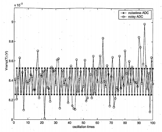
Figure 4. Servo-loop oscillations for noiseless and noisy systems. Image used courtesy of Z. Zhao
The signal averaging technique is normally applied to reduce the noise effect on test results. Two main factors that determine the feedback loop dynamics are the step size (ΔV) and the noise level present in the system. In the next article in this series, we’ll discuss how different parameters are affected by these two factors.
ADC Kickback Noise
The sample-and-hold (S/H) within the ADC basically consists of a switch and a sampling capacitor. When the switch closes at the beginning of the ADC sampling phase, the sampling capacitor shares its stored charge with the preceding drive circuitry. In the example depicted in Figure 2, the internal sampling capacitor shares its charge with C2. This causes a disturbance, known as the kickback noise, at the ADC input at the beginning of the sampling phase. This effect is illustrated in Figure 5.
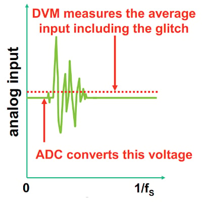
Figure 5. Image used courtesy of H. Khorramabadi
The kickback effect adds high-frequency, signal-dependent glitches to the ADC analog input. With a properly designed system, the ADC can acquire the correct sample. However, the DVM might take some samples before the glitches die out, leading to an incorrect measurement of the average value of the ADC input voltage (see Figure 5).
To reduce the kickback noise, we can increase the value of the C2 capacitor. However, this requires lowering the sampling rate (or equivalently increasing the duration of the ADC sampling phase). Therefore, by choosing C2 to be a large capacitor, we can reduce the kickback effect at the cost of a longer measurement time. If you need to brush up on these concepts, I recommend watching this video series from Analog Devices.
Alternative Servo-Loop Test Configurations
Figure 6 shows a slightly different servo-loop test configuration. In this case, rather than using current sources, the integrator input is connected to a known voltage (+V and -V in the figure) through a resistor (R). Therefore, the current delivered to the integrator is I=V/R.
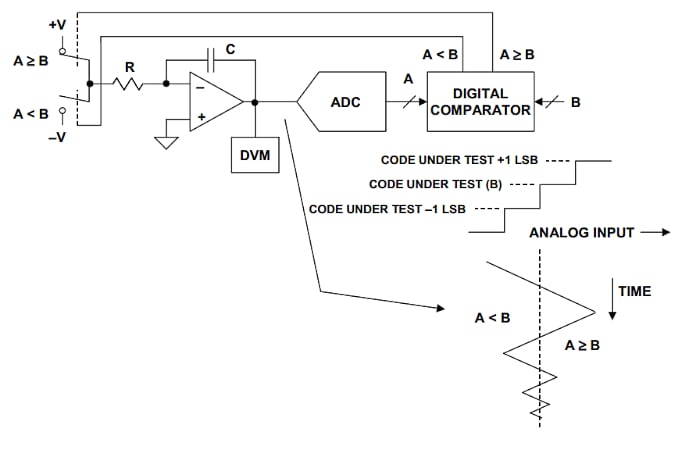
Figure 6. Alternate servo-loop test configuration using voltage sources. Image used courtesy of Analog Devices
It’s worth mentioning that the qualitative waveform provided in the figure seems incorrect because the triangular waveform has a decaying amplitude in this case, which is not consistent with typical waveforms such as those provided in Figures 3 and 4.
Another version of the servo-loop testing is shown in Figure 7. In this case, the analog integrator is replaced with a digital accumulator that adds or subtracts a specific value (N1) from its previous value, depending on the comparator output.
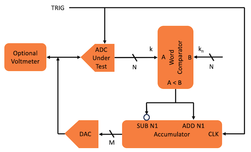
Figure 7. Alternate servo-loop test configuration with digital accumulator. Image adapted from and used courtesy of S. Max (subscription required)
Also, a DAC is used to convert the accumulator output to an analog value. This analog value that produces an estimate of the transition point is delivered to the ADC input just as it was in the diagram of Figure 2. The simulation waveforms provided in Figure 3 correspond to the configuration in Figure 7.
In the next article in this series, we’ll continue this discussion and see how different parameters of this test setup can be chosen based on the required measurement accuracy and the noise present in the system. Hopefully, you now understand the basics of servo-loop ADC testing and have even come to some level of appreciation for the difficulties of ADC characterization.
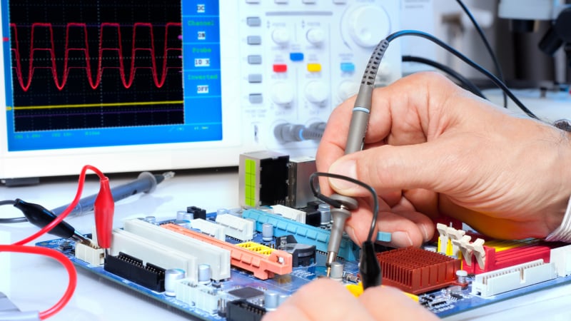
Featured image used courtesy of Adobe Stock
Related Content


Are they other test methods for modern ADCs?
How can I test a 24 or 32bitADC?
It is not only mater of test time. Longer test time envolves problems with 1/f noise.
Another issue is that 1LSB steps are so small lest say tens of nV.