Facebook
 Google
 GitHub
 Linkedin
Learn About SAR ADCs: Architecture, Applications, and Support Circuitry
In this article, we’ll first review the basic architecture of a SAR ADC and then take a look at one of its common applications.
Successive approximation register (SAR) ADCs are commonly used data converters with moderate sample rates (up to about 15 MSPS) and medium resolutions (up to about 18 bits). These structures are efficient and easy to understand. Unlike a pipelined ADC, the SAR architecture doesn’t have latency. The relatively high sample rate along with zero-latency makes the SAR ADC suitable for multiplexed data acquisition.
In this article, we’ll first review the basic architecture of a SAR ADC and then take a look at one of its common applications.
Architecture of an SAR ADC
The algorithm that a SAR ADC performs can be understood by examining the waveforms depicted in Figure 1.

Figure 1
The above waveforms illustrate the operation of a three-bit SAR ADC. During the sampling phase, the input value is sampled and held for the entire conversion phase. A SAR structure usually needs one clock cycle to sample the input and one clock cycle to determine every bit of its digital output. Therefore, an N-bit SAR ADC usually needs (N+1) clock cycles to digitize the input analog value. For the three-bit example above, we need a total of four clock cycles.
To determine the most significant bit (MSB) of the conversion, the ADC generates the analog value corresponding to half the full-scale value \(\left ( \frac {V_{FS}}{2} \right )\) and compares it to the input sample. Depending on the result of this comparison, the MSB is obtained. In the above example, the sampled value is greater than \(\frac {V_{FS}}{2}\). Hence the MSB should be logic high.
To determine the next significant bit, the ADC compares the sampled value with \(\frac {3V_{FS}}{4}\) because the previous comparison revealed that the input is between \(\frac {V_{FS}}{2}\) and \(V_{FS} \). In our example, the analog value is less than \(\frac {3V_{FS}}{4}\) and the corresponding bit should be zero. Now the ADC generates another appropriate threshold value \(\left ( \frac {5V_{FS}}{8} \right )\) for the next comparison. This procedure continues until all the three bits of the digital output are determined. In this example, the output should be 101.
The simplified block diagram of a SAR ADC is shown in Figure 2.

Figure 2
The sample and hold (S/H) is used to store the input analog value for the conversion phase. The analog comparator compares the S/H output with the analog threshold values generated by the digital-to-analog converter (DAC). As you can see, the output of the comparator is processed by a digital block called the Successive Approximation Register (SAR). This digital block controls the threshold values that the DAC generates and will eventually output the converted digital value.
Switched Capacitor DAC
Using a comparator and an array of binary-weighted capacitors, we can efficiently implement the DAC and comparator blocks of a SAR ADC.
A three-bit example is shown in Figure 3.
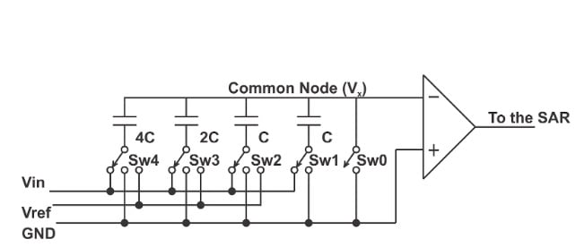
Figure 3
During the sampling phase, SW0 is closed, and the common terminal of the capacitors (Vx) is connected to ground. In this phase of operation, the other terminal of the capacitors is connected to the analog input (Vin). Hence the input signal is sampled onto the parallel combination of all the capacitors in the array.
During the conversion phase, SW0 is open. Assuming that the input impedance of the comparator is infinite, the common node of the capacitor array (Vx) is left floating (it doesn’t have a low-impedance path to ground or Vref). Hence, the total charge stored in the capacitor array will remain constant during the conversion phase. However, while the total charge is constant, connecting the lower plate of the capacitors to either Vref or ground can cause charge redistribution among the capacitors. This charge redistribution will change the voltage that appears at the comparator input. For example, assume that after the sampling phase, the capacitors are connected to ground. In this case, a voltage equal to -Vin will appear at the comparator input (because the parallel combination of the capacitors has stored the input value Vin). Now, if we connect only the largest capacitor (4C) to Vref, the voltage at the input of the comparator will increase by
\[\Delta V = V_{ref} \frac{4C}{C_{total}} = V_{ref} \frac{4C}{8C}=\frac{V_{ref}}{2}\]
In this equation, Ctotal is the sum of all the capacitors in the array (for an n-bit capacitive DAC, we have: Ctotal=(1+1+2+22+...+2n-1)C=2nC). Using the superposition principle and noting that the initial voltage at the comparator input was -Vin, the new voltage applied to the comparator will be \(V_{new}=\frac{V_{ref}}{2} -V_{in}\). The comparator of Figure 3 compares this value to 0 V. This is equivalent to comparing the input value with the threshold \(\frac{V_{ref}}{2}\) (See Figure 1).
The result of this comparison determines the MSB value. The result also determines whether the MSB capacitor (4C) should be connected to Vref (MSB=1) or ground (MSB=0) for the rest of the conversion cycle. For the next significant bit, the corresponding capacitor will be connected to Vref. This will increase the voltage at node Vx by \(\frac{V_{ref}}{4}\). The comparator output at this stage will be used to determine the value of the second most significant bit. It will also determine whether the capacitor (2C) should be connected to Vref or ground during the next conversion cycles. This procedure will continue until all of the bits of the digital output are found.
Interfacing the Analog Input to a SAR ADC
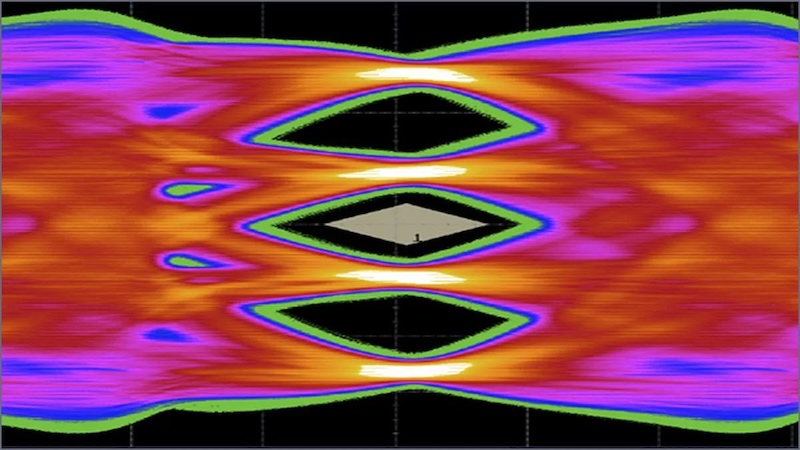
To connect the analog input to a SAR ADC, we usually need a driving amplifier and an RC filter. The amplifier acts as a low-impedance buffer and the RC filter suppresses out-of-band noise and reduces the switched-capacitor kickback of the SAR ADC inputs. Figure 4 shows the block diagram of the SAR ADC interface. The next article in this series will look at the details of designing this interface in greater detail.
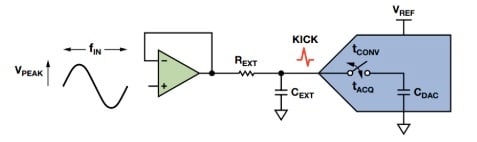
Figure 4. Image used courtesy of Analog Devices.
Common Applications
The SAR ADC is the commonly used architecture for data acquisition systems that are widely employed in medical imaging, industrial process control, and optical communication systems. In these applications, we usually need to digitize the data generated by a large number of sensors. To reduce power, size, and cost; the common approach is to multiplex the data from these sensors to a small number of ADCs. Figure 5 shows the block diagram of such a multiplexed data acquisition system.

Figure 5. Image used courtesy of Analog Devices.
The main reason for using a SAR ADC in a multiplexed data acquisition system is its fast response with no latency. Note that although the sensors connected to the multiplexer may produce low-frequency (nearly DC) signals, the multiplexer output can have rapid fluctuations. Hence, the ADC sample rate should be sufficiently high to digitize a given number of sensors. What about using other high-speed ADCs? Figure 6 below gives some typical values for the resolution and sample rate of some common ADC architectures.

Figure 6. Image courtesy of Analog Devices.
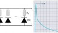
As you can see, a pipeline structure usually has a higher sampling rate, with the SAR architecture being the next high-speed structure. Although a pipeline structure can provide a higher sampling rate, it’s not suitable for a multiplexed data acquisition system because of its pipeline latency. The timing diagram of a pipelined ADC is shown in Figure 7.

Figure 7
In this example, the ADC has a latency of five clock cycles. This means that after the ADC takes a given sample, it needs seven clock cycles to process it. This pipeline delay, often referred to as latency, becomes troublesome in multiplexed applications and when the ADC is used in a “single-shot” mode. The SAR ADC has no latency and is better suited to a multiplexed data acquisition application. Besides, latency can cause serious problems when we use the data acquisition system in a closed-loop structure. In this case, the pipeline delay can lead to feedback loop instability. That’s why the SAR ADC has been a common choice for data acquisition systems for many years.
It’s worthwhile to mention that some data acquisition systems use Σ-Δ ADCs for multiplexing sensor types such as temperature, pressure, or load cells. In these cases, high resolution, accuracy, and noise performance are the key ADC factors at play. For more information, please refer to this article.
Additional Features
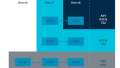
As discussed above, one of the major applications of the SAR architecture is in multiplexed data acquisition systems. To further facilitate design of these systems, many of today’s SAR ADCs have internal multiplexers and automatic channel sequencing blocks. In this way, the designer doesn’t need to get involved in creating the necessary timing and channel sequencing circuitry. An example of these SAR ADCs is shown in Figure 8.
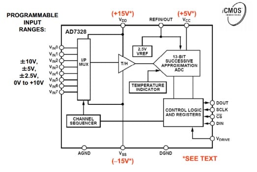
Figure 8. Image courtesy of Analog Devices.
More recent SAR ADCs try to develop techniques that reduce the switched-capacitor kickback of the inputs and increase the sampling phase duration without reducing the ADC sample rate. For more information, please refer to this article.
Conclusion
In this article, we looked at the basic architecture of a SAR ADC. We saw that unlike a pipelined ADC, the SAR architecture doesn’t have latency and offers a relatively high sample rate. These two features make the SAR ADC suitable for multiplexed data acquisition that is widely employed in medical imaging, industrial process control, and optical communication systems.
To see a complete list of my articles, please visit this page.
Related Content