Facebook
 Google
 GitHub
 Linkedin
Lossy Transmission Lines: Introduction to the Skin Effect
This article introduces high-frequency conductor losses in transmission lines caused by a phenomenon known as the skin effect.
In many applications, modeling a transmission line as a lossless structure can be a reasonably acceptable representation of the line’s real-world behavior. Such a lossless model allows us to gain insight into different properties of the transmission line. However, if we need to account for the signal attenuation, we must factor in different loss mechanisms of the transmission line.
Lossy Components in the Transmission Line Model
In a previous article, we learned about the equivalent circuit of a transmission line (Figure 1).
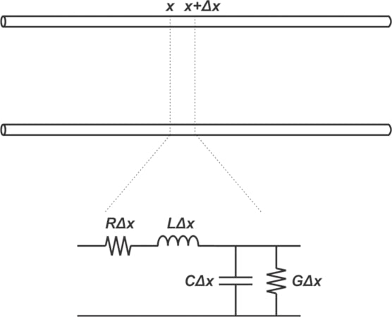
Figure 1. Lumped element equivalent circuit of a transmission line
In this model, R and G represent, respectively, the resistance per unit length of the wire and the conductance per unit length of the dielectric that separates the conductors. In order to be able to assess the conductor and dielectric losses in transmission lines, the first step is to figure out the value of R and G and how they change with different parameters. The focus of this article is evaluating the conductor resistance R.
Conductor Resistance at DC
The DC resistance per unit length of a conductor is given by the following familiar equation:
\[R_{DC}= \frac{\rho}{A} \quad \Omega /m\]
Equation 1.
where ρ is the resistivity of the conductor in Ω-m (resistivity is the reciprocal of conductivity σ); and A is the cross-sectional area of the conductor in m2. In PC boards, copper has a room-temperature resistivity of about 1.724×10⁻⁸ Ohm-m (or 6.787×10⁻⁷ Ohm-inch). Having the cross-sectional area, we can easily calculate the DC resistance. For example, a conductor of circular cross-section having a radius of r exhibits a DC resistance of
\[R_{DC}= \frac{\rho}{\pi r^2} \quad \Omega /m\]
Equation 2.
There are two conductors in a transmission line: the signal conductor and its return path. To account for the resistance of both, we can incorporate a correction factor ka into Equation 1:
\[R_{DC}=k_a \frac{\rho}{A} \quad \Omega /m\]
The value of ka depends on the structure of the transmission line. For example, if the return path is identical to the signal path, ka is equal to 2. However, in the case of a PCB trace whose return path is a wide plane, a correction factor of ka=1 can be used because the resistance of a wide plane is so low at DC (this is not the case at high frequencies where the return current mainly flows underneath the signal path).
Current Distribution at High Frequencies
At DC, the current distribution over the cross-sectional area of the conductor is uniform and the entire cross-sectional area of the conductor is equally effective in carrying current. However, as frequency increases, the current tends to flow through a shallow layer just underneath the surface of the conductor. This phenomenon, known as the skin effect, reduces the effective cross-sectional area of the conductor and hence, leads to an increase in the conductor’s AC resistance. The depth of the layer through which most of the current flows is estimated by the skin depth δ given by:
\[\delta = \frac{1}{\sqrt{\pi f \mu \sigma}}\]
Equation 3.
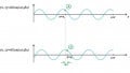
where µ is the magnetic permeability of the conductor (H/m) and σ is its conductivity in S/m. The significant result of the above equation is that the effective cross-sectional area of the conductor decreases with the square root of frequency. As a result, the high frequency resistance of a conductor is proportional to the square root of f. Figure 2 conceptually shows how the AC current is confined to the skin depth in round and rectangular conductors.
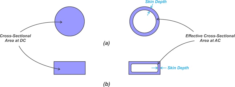
Figure 2. Skin effect in round (a) and rectangular conductors (b).
To be more accurate, the skin depth actually specifies the distance at which the current density reduces by a factor of 1/e with respect to its value at the surface of the conductor. Therefore, the current density doesn’t abruptly fall to zero after the skin depth (Figure 3).
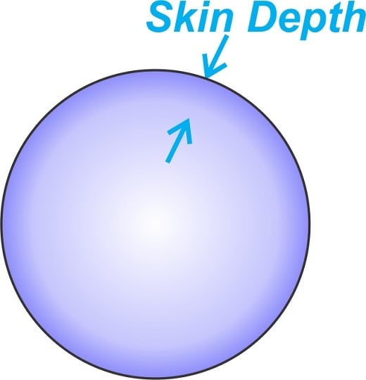
Figure 3. Conceptual illustration of current distribution in a circular cross-section conductor.
However, in order to derive some simple equations for the effective cross-sectional area of the conductor, we usually assume that the whole current is uniformly distributed in the skin depth below the conductor’s surface. In a future article, we’ll discuss in greater detail the subtleties of this approximation.
How Small Is the Skin Depth?
Equation 3 shows that the skin depth is a function of frequency as well as two material properties, namely the conductivity and magnetic permeability. For copper, substituting σ=58×106 and μ0= 4π×10-7 H/m into Equation 3 leads to a skin depth of approximately 2µm (or 0.08 mils) at 1 GHz. Table 1 gives the skin depth of copper at some other frequencies.
Table 1. Approximate skin depth for copper at various frequencies
|
f |
1 MHz |
4 MHz |
15 MHz |
50 MHz |
100 MHz |
1 GHz |
10 GHz |
|
δ (mils) |
2.6 (≈2 oz) |
1.3 (≈1 oz) |
0.67 (≈0.5 oz) |
0.37 |
0.26 |
0.082 |
0.026 |
Note that at frequencies as low as 15 MHz, the current penetration equals the 0.5 oz copper thickness. As we go to higher frequencies, the skin depth gets smaller and smaller. Keep in mind that, if we plug in different parameters of Equation 3 in the MKS system of units, the skin depth, δ, will be in meters.
Due to their high relative permeability, the skin depth of ferromagnetic metals (like nickel and iron) is much smaller than non-ferromagnetic conductors of similar conductivity. The relative permeability of nickel and iron is 100 and 1000, respectively. Figure 4 compares the skin depth vs frequency of some example metals.
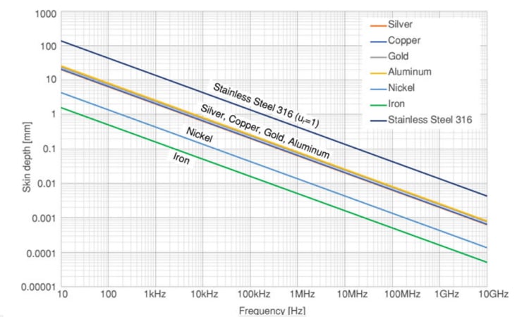
Figure 4. Skin depth as a function of frequency for assorted metals. Image used courtesy of Reto B. Keller
The skin effect manifests itself in a wide range of situations. For example, the skin effect makes long distance communication of a submerged submarine very difficult. Assuming that the seawater has typical parameters of εr=72, σ=4 S/m, and μr=1, you can verify that the seawater acts like a good conductor at 5 MHz. At this frequency, the skin depth of the seawater works out to 11.2 cm! With this small skin depth, you can calculate that the wave amplitude reduces to 1% of the transmitted value at a distance of 51.8 cm. Even at very low frequencies, the transmitted wave gets significantly attenuated.
Estimating High Frequency Resistance of a Conductor
At high frequencies, the current is mostly confined to the skin depth. Therefore, the effective cross-sectional area of a conductor can be approximated as δ times the periphery of the conductor. As an example, consider a conductor with circular cross-section having a radius of r. The effective cross-sectional area of the conductor can be approximated as 2πrδ, producing an AC resistance of
\[R_{AC}\approx \frac{\rho}{ 2 \pi r \delta} \quad \Omega /m\]
Substituting δ from Equation 3, we have:
\[R_{AC}\approx \frac{1}{ 2 r} \sqrt{\frac{\mu f}{\pi \sigma}} \quad \Omega /m\]
Equation 4.
Equating the DC resistance with the high frequency resistance of the conductor, we can define an onset frequency for the skin effect. For example, equating Equations 2 and 4, the onset frequency of the skin effect for a round conductor is found as:
\[f_{skin}=\frac{4}{\pi \mu \sigma r^2}\]
Equation 5.
Therefore, using a log-log graph, the resistance vs frequency curve for a circular cross-section conductor is as shown in Figure 4.
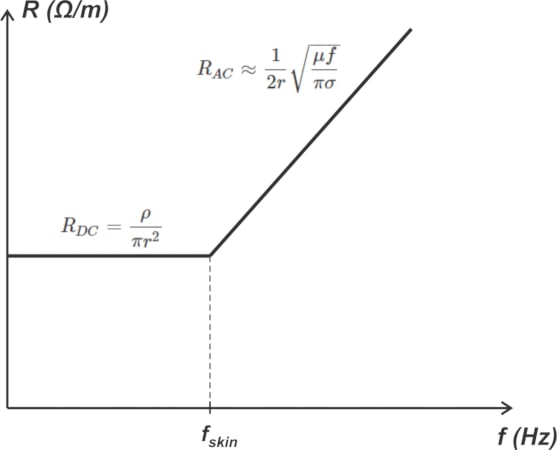
Figure 4. Resistance vs frequency for a circular cross-section conductor on a log-log graph. Image used courtesy of Reto B. Keller
While we obtained the above curve for a circular conductor, a similar behavior is observed in the resistance vs frequency curve of all conductors. Figure 5 below compares the resistance of a PCB copper trace having 0.25 mm width and 35 µm (1 oz) thickness with that of a round copper wire with diameter D=1 mm.
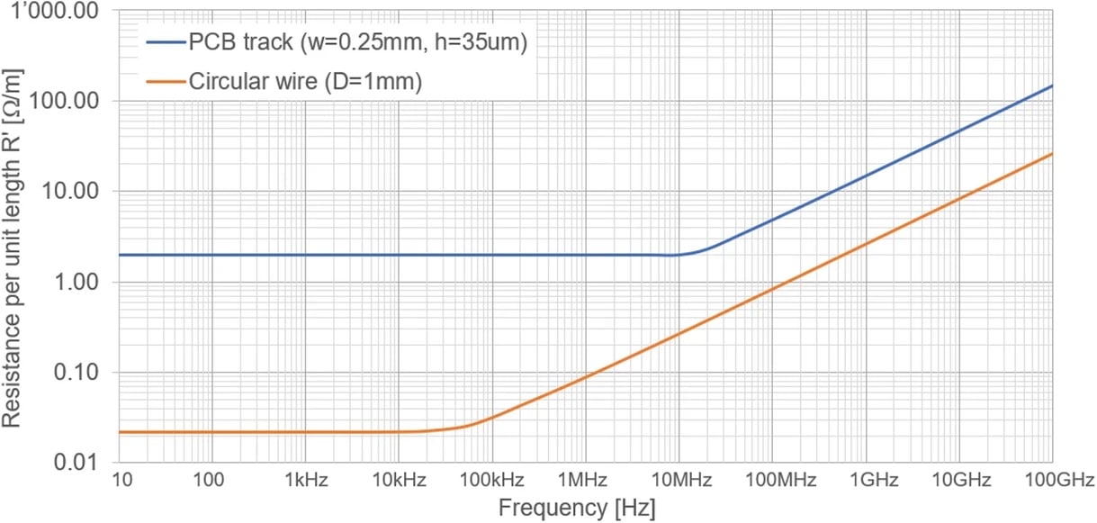
Figure 5. Resistance comparison of PCB copper trace vs round copper wire. Image used courtesy of Reto B. Keller
For a diameter of 1 mm, Equation 5 produces fskin=70 kHz, which is consistent with the orange plot. Using a similar procedure, we can derive an equation for onset frequency of the skin effect in rectangular conductors. You can find the details in Howard Johnson’s book “High Speed Signal Propagation: Advanced Black Magic”. Figure 6 shows the high frequency measured resistance of a 22-gauge copper wire loop, 1 inch in diameter.
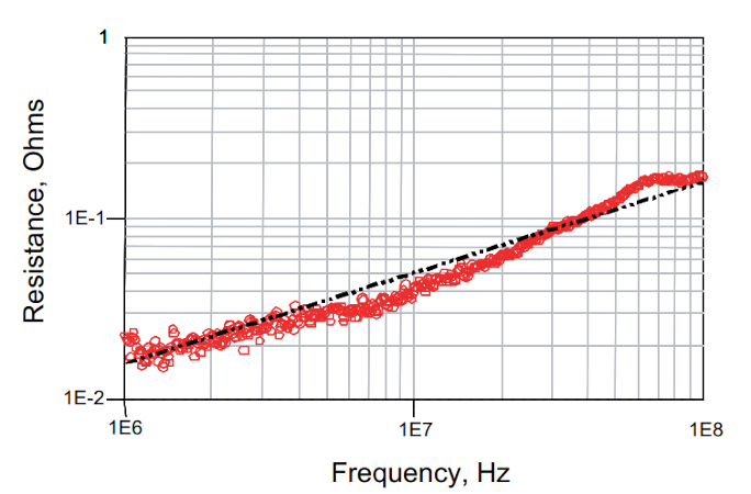
Figure 6. Measured resistance vs equation model for a copper wire. Image courtesy of Eric Bogatin.
In the above figure, the red markers correspond to the measured resistance values whereas the line corresponds to the resistance predicted by the analysis that increases with the square root of frequency. As can be seen, the measure values roughly increase with the square root of f.
Plating Microwave Components With Good Conductors
The skin depth of a good conductor is very small at microwave frequencies. Therefore, rather than using a good conductor for microwave components, we can use a bad conductor plated with a good conductor. The loss performance of the two should be similar. Plating with a highly conductive metal a couple of thousandths of an inch can completely hide the effect of the underlying bad conductor. For example, silver-plated brass waveguides can be used in place of those made of solid silver with little degradation in performance, but with much reduced material cost. You might also encounter antenna structures and RF power conductors made of hollow metal tubes that are coated with silver, for the same reason of having excellent conductivity at the “skin” of the tube.
When calculating the skin depth of plated components, it should be noted that the conductivity of a plated metal can be different from the solid form of that metal. The reason is that plated metals are porous in nature and less dense than their solid form. Also, it’s worthwhile mentioning that even microscopic scratches crossing the current flow direction can affect the effective resistance of microwave components. In a future article, we’ll continue this discussion and take a closer look at the physics behind the skin effect phenomenon.
Featured image used courtesy of Adobe Stock
Related Content