 Facebook
 Google
 GitHub
 Linkedin
How to Characterize Noise in a Custom PCB: Precision Inclinometer
Learn about the process of identifying and eliminating noise in data capture.
Learn about the process of identifying and eliminating noise in data capture.
In the previous articles, I discussed mechanical considerations, schematic design, PCB layout, and Firmware.
One of the greatest anxieties of designing a custom PCB is the testing phase.
I designed a precision inclinometer subsystem and received my brand new board. In a “Hard-way Hughes” first, the board worked on the first spin. Now it’s time to create a suitable test environment and determine the measurement resolution that the board can achieve.
This article looks at various aspects of “noise” in the device.
If you'd like to catch up on the precision inclinometer series overall, please check out the links below:
- How to Design a Precise Inclinometer on a Custom PCB (full project overview)
- Schematic Design
- PCB Layout
- Firmware Design
The Linear LTC2380IDE-24, a 24-bit ADC, was always known to be overkill for this project (the LTC2380IDE-16 is a pin-compatible replacement). My initial hope, and the “best-guess” order-of-magnitude estimate that I discussed with AAC’s Technical Director Robert Keim, was that I could statistically tease about 17-18 bits of resolution out of the device. We agreed that the best way to build this one-time board was to go with a higher-precision ADC, even if we knew we’d be throwing bits of data away. This board will never go into production, and the small increase in price of a single part is insignificant in the context of a prototype board.
The 11-bit ADC built into the SCA103T is only really useful for calibration at the factory. A 16-bit ADC would have been fine for this project, though it’s possible that under ideal conditions the sensor could provide more than 16 bits of resolution.
Understanding the Specifications: Why I Chose a 24-bit Device
The SCA103T-D04 datasheet indicates that the noise density is 0.0004°/√Hz. If we limit the bandwidth to 8 Hz, a quick multiplication of the noise density by the square root of the bandwidth indicates that the analog output resolution is in the range of 0.001°.
$$0.0004\frac°{\sqrt{Hz}} \sqrt{8\;Hz}=0.0011°$$
Calculating how many bits we can use before hitting the noise floor
However, a precision inclinometer that is used to calibrate a scientific instrument might experience very slow changes in inclination, which means that we can reduce the bandwidth (to 1 Hz, for example) and thereby decrease the noise floor.
$$0.0004\frac°{\sqrt{Hz}}\sqrt{1\;Hz}=0.0004°$$
$$\frac{30°}{2^n}=0.0004\frac{°}{\sqrt{Hz}}\sqrt{1\; Hz}$$
$$2^n=75000$$
$$n\cdot Log(2)=Log(75000)$$
$$n\approx 16.2\;\text{bits}$$
The same calculations with a reduced bandwidth. If we change the bandwidth, our bit needs also change.
In this example, a 16-bit ADC would be insufficient.
By repeating and averaging multiple measurements, I should be able to squeeze a bit more performance out of my design.
The initial prediction of a maximum resolution of 17-18 bits came from a back-of-the-envelope calculation at the beginning of the design process based on the uncertainty of measurement. The uncertainty of measurement indicates the range that a measurement lies within. For example, if we know that an object has a length between 11 cm and 13 cm, we can report the measurement as12 cm ± 1 cm, where 1 cm is the uncertainty of measurement.
The uncertainty of measurement is generally taken to be the ratio of the standard deviation to the square root of the number of measurements.
$$u=\frac{\sigma}{\sqrt{n}}$$
I won’t know the actual standard deviation until I have data, but to get an approximation, I will assume it to be in the range of 0.001°, and I’ll arbitrarily choose 1024 measurements to get an estimate of my uncertainty of measurement.
$$u=\frac{0.001°}{\sqrt{1024}}=0.0001°$$
$$Log(\frac{30°}{0.0001°})/Log(2)=18.2 bits$$
Even if I don’t need the additional bits of resolution for the conversion, I will need the additional bits of resolution for the digital averaging filter. And 16-bit ADCs don’t come with 24-bit digital averaging filters.
To be clear, 0.0001° is a practically useless and wholly unreasonable standard in most non-scientific and non-military applications. In other words, it’s a perfect-goal for “Hard-way” Hughes. To put this type of angular displacement into perspective, 0.0001° corresponds to a change in elevation of ~2 mm over a 1 km distance.
A device attempting this level of precision cannot sit on a desk because the force of a hand on the mouse will deflect the desk enough to be detected. The device cannot sit on the ground in the office next to the desk, because the weight of a person shifting in a chair will disturb the floor, as will the movement of elevators in the building, the movement of coworkers as they move around the office, etc. The PCB cannot be simply placed randomly in the room because the force of HVAC air currents on the connecting wires will provide enough force to measurably disturb the PCB. In other words, this is an unattainable goal and I’m going to spend countless hours and untold dollars of company resources trying to achieve it. I don’t want it to ever be said that I was unable to find a hundred-dollar solution to a twenty-dollar problem.
The things I can do to mitigate external effects on the device include adding mass and rigidity.
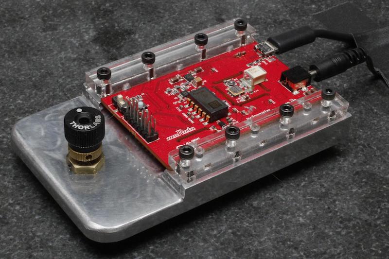
So I created a ~275 g aluminum PCB holder (~1 cm thick to provide rigidity and weight) with an adjustable differential screw mechanism.
The PCB is held rigidly in place on the board holder, and the board holder makes points of contact atop three polished round points (one differential screw and two 3mm acorn nuts) that touch a ground piece of 4″×4″×1″-thick steel plate that supports it. The polished plate sits atop a 1mm-thick piece of neoprene. That whole assembly is placed atop a 9” x 12” x 2” granite surface plate that sits atop another 1mm-thick piece of neoprene. Finally, that entire assembly sits atop an oak floor on a 4″ concrete slab.
If I had larger piece of granite, or more appropriate vibration damping material, I would have used it.

The aluminum PCB holder was placed atop a steel block that sat on a granite surface plate.
USB cables running to the device (one for the JTAG programmer, one for the data port) were taped to the granite surface plate approximately two inches from the device. The device was powered for at least 12 hours prior to data collection, allowing any thermal variations to stabilize. A FLIR TG130 thermal camera showed no thermal hot spots on the PCB. The temperature of the voltage-reference and inclinometer ICs could not be measured due to reflective package enclosures, but the sides of the IC appeared to be at the same temperature as the rest of the PCB.
Noise Characterization
The part of the circuit that I’m most concerned about is the voltage reference—so that’s the measurement I focused on first. This is the part of the circuit that I would redesign if I remade the PCB.
The sensor provides ratiometric output and the ADC has ratiometric measurement; since the same voltage reference signal is sent to both ICs, any noise in the reference itself should theoretically be self-negating. At first glance, the signal appears fine.

Tektronix MDO3104 view of the VREF net measured at test point on PCB near potentiometer.
The next image shows 0.1 V / division @ 200 ns / division. Most of the variation seems to be bound within 40 mV. And with the way the test point is attached to the board, it is impossible to know if that is indeed fluctuating voltage, or RF energy absorbed by the probe.

So far, so good, right? Perhaps. But until we enable “normal” triggering mode and set the scope to single-shot capture, we won’t know if there are any anomalies.
So I set the scope to single-shot mode and let it run for several seconds. And eventually, I picked up a hiccup.

That hiccup repeats periodically (~10 second interval) while the device is running.
Unfortunately, I don’t have enough test-points on my PCB to find any event that accompanies the noise. Noise like this doesn’t magically appear—there is always a source. Additional test points might allow me to see a correlation between the noise and the SPI or UART lines, or the wall wart power supply, or perhaps the fluorescent lights near my desk. I investigated a noise source once that turned out to coincide with the building’s AC compressor motor.
If this board was ever meant for production, I would certainly need to find out what's going on. If the noise occurs every time an SPI transaction or UART transmission occurs (it doesn’t), then the noise doesn’t really matter since the sensor measurement does not occur during those times. If the noise occurs during the SAR data acquisition phase, it’s going to be a big problem. The next article in the series will present data captured by the device in greater detail. The resolution of the data was such that this noise was clearly not affecting the sensor in any meaningful way.
Conclusion
The test points that I did include on the board showed that the noise on the PCB was quite low. While I did detect a spurious event on VREF, I could not locate where it originated. If I were to redesign the board, I would provide more taps, and coaxial taps to watch sensitive aspects of the board (such as the inclinometer outputs and the VREF inputs).
Related Content


You write “...or RF energy absorbed by the probe”. What actually is the probe? How and where is it connected? This is a much needed information that should be carefully descirbed with the measurement.
I was looking for ways to measure noise in circuit - mainly reference and power supply, but there is little information about how to best do it. I got nice results measuring PSU noise with just a piece of coax straight into the 1Meg input of the scope, with not much of common mode issues.
You have your blips in the tens of MHz range, so I guess a series 50 ohm resistor and 50ohm termination in the scope would be the better way, but for higher voltages the scope can´t hadle that, and you would need a rather large decoupling capacitor. Could you make an article about that?