Facebook
 Google
 GitHub
 Linkedin
How to Program an MSP430 Microcontroller to Gather Data from an Inclinometer
This article goes over the design of firmware for a custom PCB project: a precision inclinometer subsystem.
This article goes over the design of firmware for a custom PCB project: a precision inclinometer subsystem.
I recently designed a custom PCB with a muRata SCA103T-D04 inclinometer IC. My goal was to build a subsystem with truly ridiculous precision, able to accurately sense down to a thousandth of a degree of incline.
This article will cover some highlights of how I designed the firmware for the board's MSP430 microcontroller to gather and process data from the IC.
To catch up on the project overall, please check out the articles below:
- How to Design a Precise Inclinometer on a Custom PCB (full project overview)
- Schematic Design
- PCB Layout
Getting Started
It is difficult to create any electronic circuit these days without having to do some amount of programming. Unfortunately, the knowledge you gain learning to create firmware for one manufacturer isn’t necessarily applicable to another.
For this reason, it is usually a good idea to purchase an evaluation board so you can learn to program your microcontroller on a board that is sure to be functional before you tear your hair out with your own design. It’s also a good idea to familiarize yourself with the resources the manufacturer has made available to you—forums, datasheets, user guides, videos, etc.
In this case, I used the MSP430FR2633 so I practiced on the MSP CapTIvate MCU dev kit and turned to TI's E2E community for advice.
This article does not cover each line of the source code; rather, it provides general information about firmware programming using the source code as an example.
Adding an ASCII Pinout Diagram
Finally, I want to add some extra reference for myself. Since this is a custom board, I want to provide as much information to myself in one location as possible. There’s a very good chance I won’t remember what my pin connections are an hour from now, and I certainly won’t remember a week from now. If I make any programming changes, it would be nice to not have to dig up the schematics.
For that reason, I included a connection diagram in the source code. There are a variety of ASCII diagram generators available on the web that make this a relatively quick operation.
//   CP2102N           ┌──────┬──────┐            ┌────────────┐
// ┌────────────┐      │      │ P1.0 │→ UCB0STE  →│ EN (NC)    │
// │    USB     │→ RX →│ P2.5 │ P1.1 │→ UCB0CLK  →│ CLK        │
// │    TO      │→ TX ←│ P2.6 │ P1.2 │→ UCBSIMO  →│ SIMO (NC)  │
// │   UART     │      │      │ P1.3 │← UCBSOMI  ←│ SOMI       │
// └────────────┘      ├──────┼──────┤            │            │
//             ST_IN1 ←│ P2.0 │ P2.4 │← BUSY     ←│ BUSY       │
//             ST_IN2 →│ P2.1 │ P3.0 │→ RDL      →│ RDL        │
//                     │      │ P3.1 │→ CNV      →│ CNV        │
//                     └──────┴──────┘            └────────────┘
//                       MSP430FR2633                 ADC
The first thing we'll need to do is deal with our pins so the compiler knows which devices are connected to what. To do that, you'll need to understand the concept of registers. If you're already familiar with these concepts, feel free to jump to the "Defining Register Description Shortcuts" below.
What Are Registers?
Registers are locations in memory identified by hexadecimal numbers, and the bits belong to the register. The bits in each register control a specific aspect of the functionality of the microcontroller.
Each register controls either a byte (8 bits) or a word (16 bits). To keep the discussion simple, however, the following diagrams illustrate registers that control a single byte.

Defining Register Description Shortcuts
Now that we have an extremely brief background on registers, let's use it in context.
The register descriptions in the MSP430FR2xx Family User’s Guide indicate which bits control which functions. When a register does not allow direct access to individual bits, you can use byte operations in conjunction with an appropriate bitmask; individual bits can be set using the “|=” operator, cleared using the “&=” operator, or toggled using the “^=” operator.

The above diagram shows data in imaginary registers W, X, Y, and Z before and after four types of byte operations.
The configuration bits are provided in the datasheets in either hexadecimal or binary notation. However, it is rather inconvenient to type things such as 0x3F2A &= 0xC9 and keep track of what is happening in a program. So register and pin names are defined in referenced header files or at the beginning of the program. And the names of the register and the pins associated with that register are used instead of the raw hexadecimal and binary numbers. For example, “WDTCTL = WDTHOLD” (WatchDog Timer ConTroL register = WatchDog Timer HOLD value)—in other words, stop the watchdog timer.
So, instead of using hexadecimal addresses, programming becomes a matter of specifying registers and bits using these named shortcuts and modifying bits either directly or by using byte operations (such as those mentioned above).
void main(void)
{
    WDTCTL = (WDTPW | WDTHOLD);         // Stop watchdog timer
    …
    CSCTL3 |= SELREF__REFOCLK;          // Set REFO as FLL reference source
    CSCTL0 = 0;                         // clear DCO and MOD registers
    CSCTL1 &= ~(DCORSEL_7);             // Clear DCO frequency select bits first
    CSCTL1 |= DCORSEL_5;                // Set DCO = 16MHz
    …
Naming Variables—Bit Position of Pins
For the MSP430, each port controls a collection of pins—GPIOs are usually eight bits so that one port corresponds to one byte. While you cannot immediately define the port, the registers that control the port pins are not bit addressable and, consequently, it is not possible to create a name that corresponds to an individual pin (e.g., “#define somePinVar 1.5”).
Instead, we attach a name to the bit position of the pin and use this name in conjunction with the port register to control it.
Start by naming the pins (the port they are attached to will be stated later in the program). This is done either at the beginning of the main program or in a separate header file. The names of variables and constants are chosen to make them understandable later and are based off of corresponding net names on the PCB.
#define UART_RX_PIN     BIT5            // P2.5 eUSCI_A1
#define UART_TX_PIN     BIT6            // P2.6 eUSCI_A1

#define SPI_EN_PIN      BIT0            // P1.0 eUSCI_B0 -- not used
#define SPI_CLK_PIN     BIT1            // P1.1 eUSCI_B0
#define SPI_MOSI_PIN    BIT2            // P1.2 eUSCI_B0 -- not used yet
#define SPI_MISO_PIN    BIT3            // P1.3 eUSCI_B0

#define ADC24_RDL       BIT0            // P3.0 set low always
#define ADC24_CNV       BIT1            // P3.1 L->H->L (20 ns) to convert
#define ADC24_BUSY      BIT4            // P2.4 goes low after conversion

#define ST_IN1          BIT0            // 3PST switch input 0
#define ST_IN2          BIT1            // 3PST switch input 1
The next part of the program defines the variables used as well as the function prototypes. I used global variables and left the array as volatile to avoid any potential issues with the SPI and UART interrupt service routine. All variables defined in this section are available to all functions.
// Variable Declarations
…
uint16_t numTrials;                     // number of times to repeat reads
uint16_t numReads;                      // number of conversions per read
…
uint8_t byteCounter;                    // need 24 bits + 16 bits (5 bytes)
volatile uint8_t dataBuffer[5];         // Holder for all SPI data

// Function Prototypes
void readADC(uint16_t);                 // Runs conversions
uint8_t spix(uint8_t);                  // SPI interface communication
void uartx(uint8_t);                    // UART interface communication one-way
Assigning Pin Functions
The MSP430FR2633 has pins that can support multiple functions. So the MCU has to be told if a pin will be used for generic input/output or for an integrated peripheral such as UART or I2C.
The following several lines of code configure port 2 for use by first selecting the alternate function (i.e., the integrated peripheral) for the port 2 pins corresponding to the UART Tx/Rx connections, then configuring the UART_TX pin and the two self-test switch pins as outputs.
    // Select module function for UART (page 63)
    P2SEL0 |= (UART_TX_PIN | UART_RX_PIN);
    // Set port pins as output for UART and SP3T Switch
    P2DIR |= (UART_TX_PIN | ST_IN1 | ST_IN2);
Custom Functions
Custom functions are used to read the ADC—essentially just toggling the start-conversion flag, waiting for the busy indicator to turn off, and then toggling the start-conversion flag again—as many times as dictated by a constant set at the beginning of the program.
void readADC(uint16_t numReads)
{
// Start conversion, wait for busy flag to turn off,
// and start the next conversion.
    for (counter = 1; counter <= numReads; counter++)
    {
        P3OUT ^= ADC24_CNV;     // Toggle convert flag high > 20 ns to start
        __delay_cycles(1);      // measurement.  1/16MHz * 1 cycles = 62.5 ns
        P3OUT &= ~ADC24_CNV;    // Set convert flag back low
// Wait to let conversion finish - might never enter function
        while ((P2IN & ADC24_BUSY))
        {
            __delay_cycles(1);     // 1/16Mhz = 62.5 ns
        }
    }
Gathering Data
The data is going to come out of my microcontroller and be transmitted to a PC via USB—in a big hurry. If I converted this data to a decimal equivalent or degrees/minutes/seconds before sending it out through the UART-to-USB converter, it would be difficult to see how stable the data is as it scrolls by at ~100 lines a second. Instead, we'll convert the data to binary.
By converting the data to binary, I can quickly see in my serial monitor how many unchanged bits there are by simply counting from the left. Once the bits start changing, I’ve encountered noise (assuming, of course, that the sensor is perfectly stationary). The data comes out in blocks that I separated with the tab character in the complete program: three bytes for the angle data, two bytes for the number of samples per read (I later added two more bytes to create a counter).
    for (byteCounter = 0; byteCounter < 5; byteCounter++) //0,1,2,3,4
    { for (bitCounter = 0; bitCounter < 8; bitCounter++)
        { if (((dataBuffer[byteCounter] >> (7 - bitCounter)) & 0b1) == 0)
            { uartx('0'); // ASCII 0 }
            Else { uartx('1'); // Ascii 1 }
        }
You’ll notice that I had to change the “endianness” of each byte so that it arrives at the UART MSB first.

Sample data shows a column for the ADC reading, the number of readings taken since the last data transfer, and a counter.
Processing Data with Mathematica
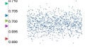
In the final program, I eventually added a trial counter and processed the data with Mathematica (free on the Rasbian OS). A future article will explain the data and data-processing in greater detail.

Data from a preliminary trial is shown above. The vertical scales with the multicolored triangles show maximum, +1σ, mean, -1σ, and minimum values at three zoom levels. A scatterplot, as well as a histogram and its accompanying idealized normal distribution, is also included.
This article explains a small part of the firmware programming for this project. The next article will characterize the noise in the device and future articles will analyze the data.
Below you'll find a downloadable file for the complete source code of the program on the MCU. Let me know in the comments below if you'd be interested in access to the Mathematica source code files, as well!
Precision_Inclinometer_Firmware.zip
//         _ _          _                 _    _____ _                _ _
//   /\   | | |   /\   | |               | |  / ____(_)              (_) |
//  /  \  | | |  /  \  | |__   ___  _   _| |_| |     _ _ __ ___ _   _ _| |_ ___
// / /\ \ | | | / /\ \ | '_ \ / _ \| | | | __| |    | | '__/ __| | | | | __/ __|
/// ____ \| | |/ ____ \| |_) | (_) | |_| | |_| |____| | | | (__| |_| | | |_\__ \
//_/    \_\_|_/_/    \_\_.__/ \___/ \__,_|\__|\_____|_|_|  \___|\__,_|_|\__|___/
//                      _____         _         __    _____         _
//                     |     |___ ___| |_    __|  |  |  |  |_ _ ___| |_ ___ ___
//                     | | | | .'|  _| '_|  |  |  |  |     | | | . |   | -_|_ -|
//                     |_|_|_|__,|_| |_,_|  |_____|  |__|__|___|_  |_|_|___|___|
//                     w/ support by Bruce McKenney            |___|  2018/11/09
//            _ __
//           ' )  )   _/_
//  ______ . ./--'__. / __.
// / / / <(_//  \(_/|<_(_/|_
//  __ __ _  ___ __   __ __ _  __  _  _ ____ ____ ____ ____
// (  |  ( \/ __|  ) (  |  ( \/  \( \/ |  __|_  _|  __|  _ \
//  )(/    ( (__/ (_/\)(/    (  O ) \/ \) _)  )(  ) _) )   /
// (__)_)__)\___)____(__)_)__)\__/\_)(_(____)(__)(____|__\_)
//
/****************************** Connection Diagram ****************************/
//   CP2102N           ┌──────┬──────┐            ┌────────────┐
// ┌────────────┐      │      │ P1.0 │→ UCB0STE  →│ EN (NC)    │
// │    USB     │→ RX →│ P2.5 │ P1.1 │→ UCB0CLK  →│ CLK        │
// │    TO      │→ TX ←│ P2.6 │ P1.2 │→ UCBSIMO  →│ SIMO (NC)  │
// │   UART     │      │      │ P1.3 │← UCBSOMI  ←│ SOMI       │
// └────────────┘      ├──────┼──────┤            │            │
//             ST_IN1 ←│ P2.0 │ P2.4 │← BUSY     ←│ BUSY       │
//             ST_IN2 →│ P2.1 │ P3.0 │→ RDL      →│ RDL        │
//                     │      │ P3.1 │→ CNV      →│ CNV        │
//                     └──────┴──────┘            └────────────┘
//                       MSP430FR2633                 ADC
/********************************* Description ********************************/
// by Mark Hughes for AllAboutCircuits.com.  Find complete information for this
// project at http://allaboutcircuits.com/author/mark-hughes
// This is a one-directional SPI to UART to USB bridge interface
// CNV is toggled one/multiple times (up to 65535) and data is averaged inside
// the ADC until SPI_CLK toggles data out and into MSP430.  Data is then sent
// via UART to CP2102N at 115200, and then from the CP2102N to the computer.
// The data is sent over UART in Binary format MSB first using ASCII characters.
// self-test and auto-calibration not yet implemented.
// When ST_IN1 != ST_IN2, enters self-test mode for sensor
/*********************************** Headers **********************************/
#include <msp430.h>
#include <driverlib.h>
#include <stdio.h>

/******************************* Pin Definitions ******************************/
#define UART_RX_PIN     BIT5            // P2.5 eUSCI_A1
#define UART_TX_PIN     BIT6            // P2.6 eUSCI_A1

#define SPI_EN_PIN      BIT0            // P1.0 eUSCI_B0 -- not used
#define SPI_CLK_PIN     BIT1            // P1.1 eUSCI_B0
#define SPI_MOSI_PIN    BIT2            // P1.2 eUSCI_B0 -- not used yet
#define SPI_MISO_PIN    BIT3            // P1.3 eUSCI_B0

#define ADC24_RDL       BIT0            // P3.0 set low always
#define ADC24_CNV       BIT1            // P3.1 L->H->L (20 ns) to convert
#define ADC24_BUSY      BIT4            // P2.4 goes low after conversion

#define ST_IN1          BIT0            // 3PST switch input 0
#define ST_IN2          BIT1            // 3PST switch input 1

/**************************** Variable Declarations ***************************/
// Can be consolidated and revised later with proper function calls and
// data returns later on.
uint8_t bitCounter;                     // 0-7 counter for bits in a byte.
uint8_t byteCounterSPI;                 // 0-4 counter for SPI data bytes.
uint8_t byteCounter;                    // need 24 bits + 16 bits (5 bytes)
uint16_t counter;                       // Temporary counter
uint16_t numTrials;                     // Temporary counter
uint16_t numTrialsMax = 1024;           // Number of times to repeat measurement
uint16_t numReads = 4;                  // number of conversions per read.

// Can replace volatile buffer with pointer later on.
volatile uint8_t dataBuffer[5];         // Holder for all SPI data

/****************************** Function Prototypes ***************************/
// Function Prototypes
void readADC(uint16_t);                 // Decides number of conversions
uint8_t spix(uint8_t);                  // SPI interface
void uartx(uint8_t);                    // UART interface

/******************************** Main Program ********************************/
void main(void)
{
    //********************* Begin Configuration ********************************

    WDTCTL = (WDTPW | WDTHOLD);         // Stop watchdog timer
    FRCTL0 = FRCTLPW | NWAITS_1;        // FRAM configuration for > 8 MHz
    __bis_SR_register(SCG0);            // Disable Frequency Locked Loop (FLL)
    CSCTL3 |= SELREF__REFOCLK;          // Set REFO as FLL reference source
    CSCTL0 = 0;                         // Clear DCO and MOD registers
    CSCTL1 &= ~(DCORSEL_7);             // Clear DCO frequency select bits first
    CSCTL1 |= DCORSEL_5;                // Set DCO = 16MHz
    CSCTL2 = FLLD_0 + 487;              // DCOCLKDIV = 16MHz
    __delay_cycles(3);                  // Wait to allow stabilization of clock
    __bic_SR_register(SCG0);            // Reenable FLL
    while (CSCTL7 & (FLLUNLOCK0 | FLLUNLOCK1))
        /*EMPTY*/;            // FLL locked
    // default DCOCLKDIV as MCLK and SMCLK source
    CSCTL4 = SELMS__DCOCLKDIV | SELA__REFOCLK;
    // Disable GPIO power-on default high-impedance mode
    PM5CTL0 &= ~LOCKLPM5;   // Disable GPIO power-on default high-impedance mode
    // PxDIR: 0(In) 1(Out)
    // PxSEL: Function Select Register (see datasheet)
    // PxOUT: 0(L) 1(H): Output Register
    // PxREN: 0(L) 1(En): Resistor Enable (on input only)

    // Select SPI module function for SPI (page 60)
    P1SEL0 |= (SPI_MISO_PIN | SPI_MOSI_PIN | SPI_CLK_PIN);
    // Set MOSI and CLK as outputs.
    P1DIR |= (SPI_MOSI_PIN | SPI_CLK_PIN);

    // Select module function for UART (page 63)
    P2SEL0 |= (UART_TX_PIN | UART_RX_PIN);
    // Set port pins for UART and SP3T Switch
    P2DIR |= (UART_TX_PIN | ST_IN1 | ST_IN2);
    // IN1/IN2 initially low to open SPST switch.
    P2OUT &= ~(ST_IN1 | ST_IN2);

    // Set port pins for ADC
    P3SEL0 &= ~(ADC24_RDL | ADC24_CNV);
    // Set direction for RDL and CNV
    P3DIR |= (ADC24_RDL | ADC24_CNV);
    // Set port output low for RDL and CNV
    P3OUT &= ~(ADC24_RDL | ADC24_CNV);

    // Setup SPI in UCB0 Control Word 0
    // Place UCB in reset state before modifying settings

    UCB0CTLW0 |= UCSWRST;
    // Master-mode, synchronous clock, inactive state high, MSB first.
    UCB0CTLW0 |= (UCMST | UCMSB | UCCKPH | UCSYNC | UCMSB | UCSSEL__SMCLK);
    // Bit clock prescaler
    UCB0BRW = 0x0002;   // Bit rate clock = SMCLK/2 = 8 MHz
    // Release reset and initialize state machine
    UCB0CTLW0 &= ~UCSWRST;

    // Put UCA state machine in reset, select mode and clock.
    UCA1CTLW0 = UCMODE_0 | UCSSEL__SMCLK | UCSWRST; // UART, SMCLK, Reset
    // 16M/(UCOS)16/9600 UCA1BRW = 104
    // UCA1BRW = 104;
    // UCBRS=0xD6, 16x oversample, UCBRF=2
    // UCA1MCTLW = (0xD6 << 8) | UCOS16 | UCBRF_2;
    // 16M/(UCOS)16/115200 UCA1BRW = 8;
    UCA1BRW = 8; // 115200 Baud.
    UCA1MCTLW = (0xD6 << 8) | UCOS16 | UCBRF_11;  // 115200 Baud.

    // Release reset and initialize state machine
    UCA1CTLW0 &= ~UCSWRST;

    /**************************** End Configuration ***************************/

    /****************************** Main Program ******************************/
    // Read the ADC a certain number of times.  Toggle ST_IN1 and ST_IN2 to
    // flash LED after certain number of reads.
    for (numTrials = 1; numTrials <= numTrialsMax; numTrials++)
    {
        // Turn LEDS on/off every 100 trials
        if (numTrials % 100 == 1)
        {
            P2OUT ^= (ST_IN1 | ST_IN2);
        }
        __delay_cycles(1);
        readADC(numReads);              // Perform n conversions
    }
    // Turn LEDS off because numTrials likely didn't.
    P2OUT &= ~(ST_IN1 | ST_IN2);

    // Add an additional carriage return and newline.
    uartx('\r'); // Carriage return
    uartx('\n'); // Newline
// End main.
}

/**************************** Function to read ADC ****************************/
void readADC(uint16_t numReads)
{
// Start conversion, wait for busy to turn off, and start the next conversion.
    for (counter = 1; counter <= numReads; counter++)
    {
        P3OUT ^= ADC24_CNV;     // Toggle convert flag high > 20 ns to start
        __delay_cycles(1);      // measurement.  1/16MHz * 1 cycles = 62.5 ns
        P3OUT &= ~ADC24_CNV;    // Set convert flag back low

        // Wait to let conversion finish - might never enter function
        while ((P2IN & ADC24_BUSY))
        {
            __delay_cycles(1);     // 1/16Mhz = 62.5 ns
        }
    }

    // Shift out dummy bytes to allow ADC data to shift into dataBuffer[]
    for (byteCounterSPI = 0; byteCounterSPI < 5; byteCounterSPI++)
    {   // Shift out useless data to allow shift in of ADC data.
        dataBuffer[byteCounterSPI] = spix(0xFF);
    }

    // Find binary equivalent of each dataBuffer byte.  Send it out over UART.
    // Each byte is shifted to the right n-bits and the LSB is read as 1 or 0
    // (7 - bitCounter) is used to change Endianess.
    for (byteCounter = 0; byteCounter < 5; byteCounter++) //0,1,2,3,4
    {
        for (bitCounter = 0; bitCounter < 8; bitCounter++) //0,1,2,3,4,5,6,7
        {
            // Need to change endianness of data before sending out UART
            if (((dataBuffer[byteCounter] >> (7 - bitCounter)) & 0b1) == 0)
            {
                uartx('0'); // ASCII 0
            }
            else
            {
                uartx('1'); // Ascii 1
            }
        }

        // Data Formatting
        if (byteCounter == 2)
        {
            // After the three data-bytes, add a tab to separate number of reads
            uartx('\t'); // Ascii tab
        }

        // After the last byte is out, send a carriage return and line feed.
        if (byteCounter == 4)
        {
            uartx('\t');

            for (bitCounter = 0; bitCounter < 16; bitCounter++)
            {
                if (((numTrials >> (15 - bitCounter)) & 0b1) == 0)
                {
                    uartx('0'); // ASCII 0
                }
                else
                {
                    uartx('1'); // Ascii 1
                }
            }

            uartx('\r'); // Return
            uartx('\n'); // Line Feed
        }
    }
    return;
}

uint8_t spix(uint8_t c)
{
    while (!(UCB0IFG & UCTXIFG))
        /*EMPTY*/;
    UCB0TXBUF = c;
    while (!(UCB0IFG & UCRXIFG))
        /*EMPTY*/;
    c = UCB0RXBUF;
    return (c);
}

void uartx(uint8_t c)
{
    while (!(UCA1IFG & UCTXIFG))
        /*EMPTY*/;
    UCA1TXBUF = c;
    return;

}