
Noise Figure Concepts—Power Gain, Lossy Components, and Cascaded Systems
Learn about the RF noise figure (NF), its power gain, lossy components, and cascaded systems.
The concept of noise factor is reasonably intuitive, which is to characterize the degradation in the SNR (signal-to-noise ratio) as the signal passes through the component. However, several subtleties are buried in the noise figure definition that is not sometimes highlighted enough. One intricacy that must be fully understood is that the noise figure value is specified for a known source resistance (typically 50 Ω) at a standard temperature of 290 K.
In this article, we’ll discuss another important subtlety, namely the type of power gain used in the noise figure definition. Afterward, we’ll look at the noise figure of lossy components as well as cascaded systems.
Revisiting the Noise Figure Definition and Signal-to-Noise Ratio
The noise factor (F) is defined as the ratio of the SNR at the input to the SNR at the output:
\[F=\frac{\frac{S_i}{N_i}}{\frac{S_o}{N_o}}\]
Equation 1.
Where:
- Si and So are the available signal powers at the input and output of the circuit
- Ni and No are the available noise powers at the input and output
Substituting So = GASi produces the following alternative equation:
\[F=\frac{N_o}{G_A N_i}\]
Where GA is the available power gain of the circuit.
Next, let's take a look at the definition of the available power gain.
Available Power Gain of a Module Using Impedance
Figure 1 illustrates how the available power gain of a module for a given source impedance ZS = RS + jXS is calculated.
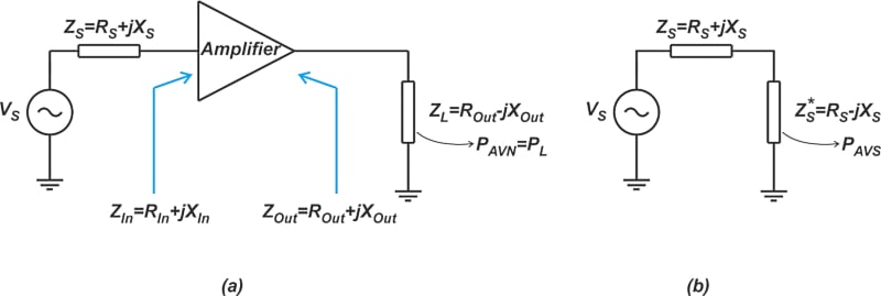
Figure 1. Diagrams showing the module's power gain for a given source impedance.
Assume that the input and output impedance of the module is ZIn = RIn + jXIn and Zout = Rout + jXout. As shown in Figure 1(a), we can connect the module output to a conjugate-matched load—i.e., ZL = Rout - jXout—and measure the power delivered to the load, PL. Since the output is conjugately matched, PL is the available power from the network PAVN.
Another quantity that is required is the available power from the source PAVS. This is the power that the source delivers to the complex conjugate of ZS, as illustrated in Figure 1(b). The ratio of PAVN to PAVS is defined as the available power gain of the module GA:
\[G_A = \frac{P_{AVN}}{P_{AVS}}\]
The available gain depends on ZS but not ZL. This is because the load impedance is, by definition, a complex conjugate match of the module’s output impedance and, thus, is already set by the module’s output impedance. Keep in mind that the available gain accounts for the mismatch between the source and the input of the DUT (device under test).
In the noise figure definition (Equation 1), Si is the available power of the signal source, and So is the output power that can be delivered into a matched load. Therefore, the ratio So / Si meets the definition of available power gain. Keep in mind that there are several different power gain definitions in RF work, such as transducer power gain and insertion power gain. If we use a power gain other than the available gain in our NF calculations, we will achieve an approximation of the actual NF value. For example, practical noise figure measurement methods most often determine the insertion gain of the DUT. The use of the insertion gain rather than the available gain can introduce errors in our noise figure measurements.
It is also worthwhile to mention that the available gain is useful when dealing with a cascade of stages. The overall available gain of a cascade is equal to the product of the individual available gains. To find the cascade’s available gain, the available gain of each stage should be specified for a source impedance equal to the output impedance of the preceding stage.
Noise Figure of Lossy Components
When designing RF systems, we occasionally find it necessary to introduce loss at a particular point of the signal chain. For example, in test and measurement applications, we can reduce mismatch uncertainty through attenuators. A passive circuit that attenuates the signal must have physical resistance, and we know that resistors produce thermal noise. Therefore, passive attenuators degrade the SNR performance. Let’s see how we can determine the noise figure of these components. As an example, consider a 6 dB T-type attenuator designed for a 50 Ω system, as shown below (Figure 2).
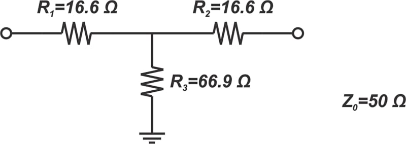
Figure 2. Example diagram for a 6 dB T-type attenuator designed for a 50 Ω system.
We can follow the general procedure and determine the noise figure of this circuit by performing a noise analysis. This method involves some tedious calculations. A more efficient method is to consider the Thevenin equivalent of the circuit. The available noise at the output of the attenuator is the available noise from the Thevenin resistance of the attenuator. As a general rule, if the Thevenin resistance seen between two terminals of a passive (reciprocal) network is equal to Rth, then the PSD of the thermal noise seen between these terminals is given by \(\overline{V_n^2}=4kTR_{th}B\). In our example, the attenuator is designed for a 50 Ω system. Adding the input and output terminations, we obtain the following schematic shown in Figure 3.
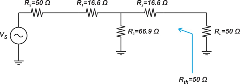
Figure 3. Diagram showing the attenuator at 50 Ω and input and output terminations.
By design, the output impedance, Rth, is equal to the reference impedance of the system, i.e., Rth = 50 Ω. Since Rth is equal to the source impedance, Rs, the noise power available at the output of the attenuator is equal to that provided by the source impedance, Rs (we’re implicitly assuming that the attenuator and Rs are at the same temperature). This means that the noise power at the input and output of the attenuator is the same or Ni = No in Equation 1, which leads to:
\[F=\frac{\frac{S_i}{N_i}}{\frac{S_o}{N_o}}=\frac{S_i}{S_o}\]
On the other hand, we know that the attenuator attenuates the input signal power by its specified value. For example, with a 6 dB attenuator, Si is 6 dB greater than So. Taking this into account, the above equation shows that the noise figure of a 6 dB attenuator is 6 dB. In general, if the physical temperature of a passive attenuator is at T0 = 290 K, then its noise figure in dB is equal to its loss in dB.
If we analyze the circuit in Figure 3, we’ll find out that the noise produced by Rs is attenuated by 6 dB as it passes through the attenuator. However, the resistors R1, R2, and R3 contribute just enough noise to the circuit output so that the total available noise at the input and output of the attenuator is the same.
What If the Attenuator Is at an Arbitrary Temperature?
The above discussion applies only to the case where the attenuator is at T0. If the attenuator is at an arbitrary temperature T, we can first consider the case where both the attenuator and the source resistance are at T. By analyzing this case, we can determine the noise added by the attenuator No(added) and can use this information to find the noise figure. Let’s examine the circuit in Figure 3 as an example. If the whole circuit, including Rs, is at T, then the available noise power at the output No is equal to that of Rs (which we know is kTB):
\[N_o=kTB\]
We can find the total output noise No through another equation:
\[N_o=N_{o(source)}+N_{o(added)}=kTBG_{A}+N_{o(added)}\]
Where:
- No(source) is part of the output noise that stems from the source impedance
- No(added) is the noise added by the attenuator
- GA is the available gain of the block
Combining these equations, we can find No(added) = kTB(1 - GA). Now, if we assume that Rs is at the standard temperature T0 as specified by the noise figure definition, the noise figure of a lossy component at T is found as:
\[\begin{eqnarray}
F&=&1+\frac{N_{o(added)}}{N_{o(source)}}=1+ \frac{kTB(1-G_A)}{kT_0BG_A} \\
&=& 1+ \frac{1-G_A}{G_A} \times \frac{T}{T_0}
\end{eqnarray}\]
For an attenuator, the loss L is equal to 1/GA, and the above equation can be a little bit simplified as:
\[F=1+(L-1)\times \frac{T}{T_0}\]
In the special case of T = T0, we get F = L, which is consistent with our discussion in the previous section.
Noise Figure of Cascaded System
While we normally characterize circuit blocks individually, we most often use them as constituent blocks of a cascaded system. Therefore, it is important to determine the noise performance of the overall system from the noise figure specification of the individual blocks. Consider a cascaded system made of N two-port devices, as shown in Figure 4.
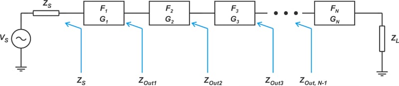
Figure 4. Example cascaded system made of N two-port devices.
In the above figure, Fi and Gi denote the noise factor and available power gain of the i-th stage. The noise factor of the cascaded system can be found by applying the following equation, known as Friis’ equation:
\[F = F_1 + \frac{F_2 - 1}{G_1} + \frac{F_3 - 1}{G_1 G_2} + \dots + \frac{F_N - 1}{G_1 G_2 \dots G_{N-1}}\]
Note that in the above equation, Fi and Gi terms are all linear (not logarithmic) quantities. According to Friis’s formula, the noise factor of each stage is divided by the total gain that precedes that stage. Therefore, the later stages have a diminished effect on the overall performance. This means that the first stage has a significant impact on the noise figure of the whole system.
In a previous article, we discussed that the noise factor metric is specified for a given source impedance. When dealing with Friis’s equation, it should be noted that the noise factor of each stage should be specified for the output impedance of its preceding stage. For example, referring to Figure 4, the noise factor of the second stage F2 should be specified for a source impedance of Zout1, F3 corresponds to a source impedance of Zout2, and so on. Let’s look at an example to clarify some of the above concepts.
Example: Find the Noise Figure of a Wireless Reciever Front End
Find the noise figure of the following wireless receiver front end, shown in Figure 5.
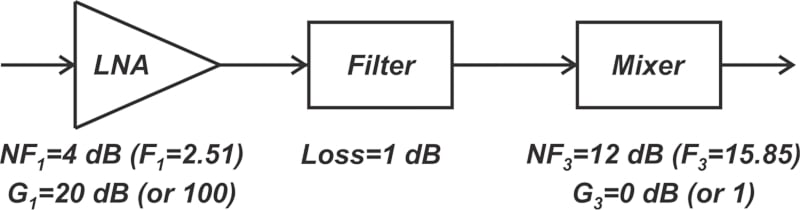
Figure 5. Example wireless receiver from end system.
The noise factor and gain of the LNA and mixer are also shown in the figure. In addition, the filter has a loss of 1 dB. We know that the noise figure of a passive attenuator in dB is equal to its loss in dB (assuming a physical temperature of T0 = 290 K). Therefore, for the filter, we have:
\[G_2 = -1 \text{ } dB = 10^{-1/10}=0.79\]
\[NF_2 = 1 \text{ } dB \Rightarrow F_2= 10^{1/10}=1.26\]
Applying Friis’s equation, we have:
\[\begin{eqnarray}
F &=& F_1 + \frac{F_2 - 1}{G_1} + \frac{F_3 - 1}{G_1 G_2} \\
&=& 2.51 + \frac{1.26-1}{100} + \frac{15.85-1}{100 \times 0.79} \\
&=& 2.7 = 4.31 \text{ } dB
\end{eqnarray}\]
Although the mixer itself has a large noise factor of F3 = 15.85, adding the filter and mixer increases the overall noise factor by a relatively small value, from 2.51 to 2.7. The contribution of the filter and mixer is small because a relatively large gain precedes these components.
Discrete vs. Integrated RF Design
Friis’s approach best suits discrete RF designs where the input and output impedance of each block is matched to a reference impedance (typically 50 Ω). In integrated RF systems, the input/output impedances of different blocks are usually unknown and different; and no attempt is usually made to provide impedance matching between the stages. In these cases, Friis’ equation becomes cumbersome; and it’s easier to find the noise figure directly by calculating the contribution of different noise sources. In the next articles in this series, we’ll discuss this in greater detail.
To see a complete list of my articles, please visit this page.


