Facebook
 Google
 GitHub
 Linkedin
Understanding the RF Noise Figure Specification
Take a closer look at the definition of the RF noise figure and discuss some subtleties to help avoid erroneous interpretations of this specification.
In RF applications, we usually deal with very weak signals that can be easily obscured by the noise generated within our circuitry. The noise level ultimately determines the minimum signal that can be reliably detected by the receiver. Therefore, noise characterization of RF components and systems is paramount. In our introductory article about a noise figure, we learned how this metric is used to characterize the noise performance of RF components.
Now that we’re familiar with the basic concepts, we can take a closer look at the definition of the noise figure and discuss some subtleties that are not sometimes highlighted enough. This should help you avoid erroneous interpretations of this specification.
The Noise Figure Definition and Noise Factor Equation
The noise factor (F) of a circuit can be defined as:
\[F=\frac{N_o}{GN_i}\]
Equation 1.
Where:
- No is the total noise at the output, including the effect of the internal noise sources within the circuit and the noise from the source impedance
- Ni is the noise the source impedance produces at the circuit's input
- G is the power gain of the stage
Although this explanation is correct, and actually similar explanations are provided in some references, such as the 4th edition of the widely used textbook “Analysis and Design of Analog Integrated Circuits” by Paul R. Gray, it doesn’t provide all the details of the noise figure definition. According to the IEEE definition, Ni is the available thermal noise power of the source resistor at a temperature of T0 = 290 K° (or 16.85 °C). This temperature is a little colder than a comfortable room temperature; however, it is sometimes referred to as the room temperature in RF work.
In addition, the IEEE definition states that No is the available noise power at the output of the device, and G is the available power gain of the device. The key points here are the reference temperature of the specification T0 = 290 K°, as well as the descriptor “available” used to describe all three parameters of the equation Ni, No, and G. In the rest of the article, we’ll discuss in detail what the implications of the “available noise power at T0 = 290 K" are.
Maximum Available Noise Power
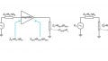
The random motion of thermally excited charge carriers manifests itself as noise in resistors. A noisy resistor can be modeled by adding a noise voltage source in series with the noiseless resistor, as shown below in Figure 1.
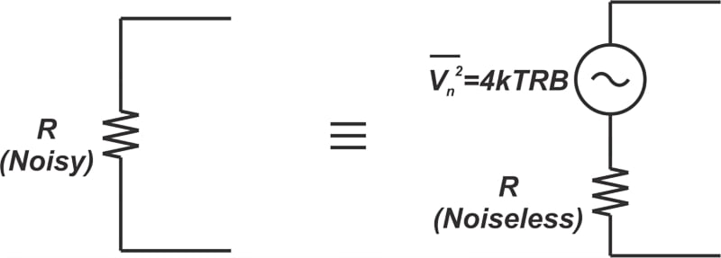
Figure 1. Example diagram of a noise resistor and adding a noise voltage source in series with a noiseless resistor.
The noise voltage source has a PSD (power spectral density) of \( \overline {V_n^2} = 4 \space kTRB\), where:
- k is Boltzmann’s constant (1.38 × 10⁻²³ Joules/Kelvin)
- T is the temperature in Kelvin
- B is the considered bandwidth (Hertz)
In the noise figure definition, Ni is the maximum available noise power of the source resistor. The question now is, what is the maximum noise power that the circuit in Figure 1(b) can provide? From basic circuit theory, we know that the maximum power is transferred when the load resistor is equal to the source resistor. Therefore, the following circuit (Figure 2) can be used to find the maximum available noise power of the source resistor, RS.
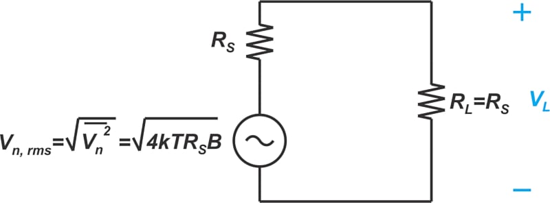
Figure 2. Diagram of a circuit used to find the maximum available noise power of the source resistor.
Keep in mind that we have used the RMS (root-mean-square) value of the noise source in the above diagram. Since half of the noise voltage appears across the load, the noise power delivered to the matched load, RL = RS, can be found by:
\[\begin{eqnarray}
P_{L} = \frac{V_{L}^2}{R_L} &=& \Big ( {\frac{V_{n,rms}}{2}} \Big ) ^2 \times \frac{1}{R_L} \\
&=& \frac{4kTR_SB}{4} \times \frac{1}{R_S} \\
&=& kTB
\end{eqnarray}\]
Equation 2.
This is an important result for noise figure calculations. Note that the available noise power is independent of the resistor value. Whether it is a 1 mΩ resistor or a 1 MΩ resistor, the available noise power is kTB. In a 1 Hz bandwidth, the available noise power is kT. The noise figure definition is based on the available noise power at T0 = 290 K. Expressing kT0 in dB, the available noise power at this reference temperature works out to -174 dBm/Hz, as calculated below:
\[10 log \big ( kT_0 \big )=10 log \big ( 1.38 \times 10^{-23} \times 290 \big ) \approx -174 \text{ } dBm\]
Noise Figure Specifies the Relative Amount of Added Noise
Since the noise figure definition is based on Ni = kT0B, it specifies the relative amount of noise that is being added to the signal with respect to Ni. Consider the following noise figure equation that we derived in the previous article:
\[F=1+\frac{N_{o(added)}}{N_{o(source)}}\]
Here, No(source) is part of the output noise that stems from the source impedance; and No(added) is part of the output noise that is produced within the circuit itself—excluding the source resistance contribution. Noting that No(source) = kT0BG, we get Equation 3:
\[F=1+\frac{N_{o(added)}}{kT_0BG}\]
Equation 3.
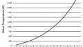
To better visualize the noise terms of the above equation, consider the following plot in Figure 3, which is sometimes referred to as the “noise line”.
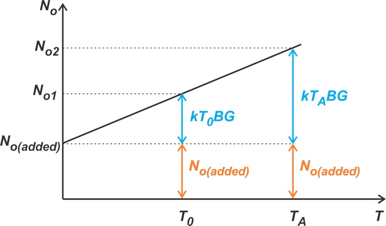
Figure 3. Plot showing a noise line.
In the above diagram, the total output noise, No, is plotted against the source resistance temperature, T. If RS were noiseless (or at T = 0 K), the only noise that appeared at the output would have been that of the device under test or No(added). As we increase the temperature of RS, its noise contribution rises. The noise figure metric, which corresponds to T = T0, actually specifies the ratio of the output noise contributed by RS at T0—i.e., kT0BG—to that of the device under test (No(added)). For instance, if the noise factor of a system is F = 2 (or NF = 3 dB), we know that No(added) is equal to kT0BG.
As the graph clearly shows, the ratio of the RS noise and No(added) is not constant and changes with T. Therefore, if RS is at a temperature other than T0, we cannot directly use the noise figure equation to find the output noise. Instead, we should first find the noise coming from the DUT (device under test), add the noise from RS at the temperature of interest, and finally calculate the total output noise.
We can also express Equation 3 in terms of the input-referred noise values by dividing both the numerator and denominator of the fraction by the power gain of the stage. This produces Equation 4:
\[F=1+\frac{N_{i(added)}}{N_{i}}\]
Equation 4.
In this equation, Ni(added) is the input-referred noise contributed by the DUT, and Ni is the available noise power of the source at 290 K. Again, if F = 2, the input-referred noise contributed by the DUT is equal to Ni = kT0B. Let’s look at an example to clarify these concepts.
Example: Using the Noise Figure Equation
The noise figure, bandwidth, and gain of an amplifier are, respectively:
- NF = 2.55 dB
- B = 10 MHz
- Gain = 5.97 dB
Assuming that the available input noise is kTAB, find the output noise for two different cases: 1 - TA = 290 K and 2 - TA = 150 K.
We first find the linear values of the noise figure and gain:
\[F=10^{\frac{NF}{10}}=10^{0.255}=1.8\]
\[G=10^{\frac{Gain}{10}}=10^{0.597}=3.95\]
Since the definition of noise figure assumes that the input noise is the available noise power at T = 290 K, we can find the output noise at this temperature directly from Equation 1:
\[N_{o}=N_{i}FG=kT_{0}B\times FG\]
Expressing the right-hand side in decibels, we have:
\[\begin{eqnarray}
N_o &=& 10 log(kT_0) + 10log(BFG) \\
&=& -174 \text{ }dBm/Hz + 10 log(10 \times 10^{6} \times 1.8 \times 3.95) \\
&=& -95.48 \text{ } dBm
\end{eqnarray}\]
For TA = 150 K, we cannot directly use the noise figure equation. However, the noise figure equation can be used to calculate the noise contributed by the system. Substituting Ni = kT0B into Equation 4, the input-referred noise contributed by the system is found as:
\[N_{i(added)}=(F-1)kT_0B\]
With F = 1.8, we obtain Ni(added) = 0.8kT0B. Therefore, the total noise at the input is:
\[N_{i(total)}=N_{i(added)}+kT_{A}B\\ =0.8kT_{0}B+kT_{A}B\]
Multiplying this value by the gain of the system, G, gives us the total output noise power. In the following equation, I write TA in terms of T0 to simplify the calculations:
\[\begin{eqnarray}
N_{o(total)}&=&G \big ( 0.8kT_0B+kT_A \frac{T_0}{T_0}B \big ) \\
&=& GkT_0B(0.8 + \frac{150}{290})
\end{eqnarray}\]
Expressing the right-hand side in decibels, we have:
\[\begin{eqnarray}
N_{o(total)} &=& 10 log(kT_0) + 10log(BG \times 1.317) \\
&=& -174 \text{ }dBm/Hz + 10 log(10 \times 10^{6} \times 3.95 \times 1.317) \\
&=& -96.84 \text{ } dBm
\end{eqnarray}\]
Without paying attention to the definition of the noise figure, one might substitute Ni = k × 150 × B into Equation 1, which produces the incorrect result of No = -98.34 dBm.
Physical Temperature or Noise Temperature
In the above discussion, we highlighted the impact the physical temperature of the source resistance, RS, can have on our NF calculations. More often than not, the driving-point impedance (RS) is at the same physical temperature as the DUT; however, the input noise power that the circuit receives is higher than kT0B. This commonly occurs in cascaded systems where the noise floor is increased by each block in the signal chain. As a result, the input noise of the downstream stages in a cascade normally exceeds kT0B. In these cases, again, we cannot find the output noise level by directly applying the noise figure equations. Instead, we can first use the NF equation to find the noise the circuit produces (Ni(added)) and then use that information along with the input noise level to find the total output noise. Additionally, it is also helpful to define an equivalent noise temperature Te for the input noise. This is the temperature where the available thermal noise power (kTeB) is equal to the input noise power. If the input noise power is N1, its equivalent noise temperature is:
\[T_{e}=\frac{N_1}{kB}\]
The noise figure and equivalent noise temperature are interchangeable characterizations of the noise properties of a component. In the next article, we’ll look at examples of using the noise temperature concept.
Noise Figure Specifies the SNR Degradation
The noise figure is a direct measure of the SNR (signal-to-noise ratio) degradation caused by the circuit. This statement is correct; however, it deserves a bit more explanation. Let’s consider the example we discussed above one more time. There we assumed that the noise figure and gain of the system are NF = 2.55 dB and Gain = 5.97 dB, respectively, and assume that the input signal power is -40 dBm. When RS is at TA = 290 K, the input noise power is:
\[\begin{eqnarray}
N_i &=& 10 log(kT_0) + 10log(B) \\
&=& -174 \text{ }dBm/Hz + 10 log(10 \times 10^{6}) \\
&=& -104 \text{ } dBm
\end{eqnarray}\]
From the example's results, we know that the output noise power is -95.48 dBm. The signal and noise powers at the input and output for this example are summarized in Figure 4.
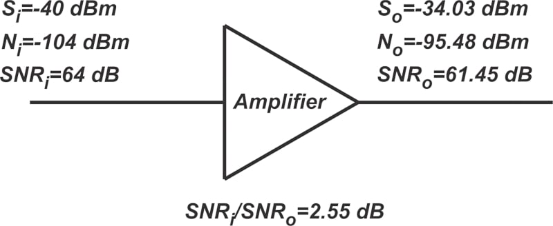
Figure 4. Summarization of the signal and noise powers at the input and output for our earlier example.
The output signal power is found by multiplying the input signal by the power gain of the amplifier. Figure 4 also provides the input and output SNR, as well as the SNR degradation. Note that the ratio SNRi / SNRo is equal to the noise figure NF = 2.55 dB, which is no big surprise because we know that this ratio is actually the definition of the noise figure. However, what about the case of TA = 150 K? In this case, the input noise is Ni = -106.86 dBm. The results from the previous example are summarized in Figure 5.
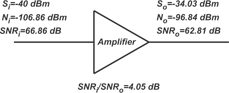
Figure 5. Another summarization of results for the above example.
As you can see, the SNR degradation (SNRi / SNRo) is now greater than the NF. This is because the input noise is less than the standard value, making the noise contribution of the amplifier more significant. Therefore, the noise figure determines the SNR degradation when the input noise is kT0B. For example, if a circuit has a noise figure of 7 dB and the input noise power of the block is kToB, then the SNR at the output of that block is 7 dB less than the input SNR.
In the next article, we’ll continue this discussion and learn about the “available gain power” that appears in the NF definition.
To see a complete list of my articles, please visit this page.
Related Content