Facebook
 Google
 GitHub
 Linkedin
Mismatch Loss and Mismatch Uncertainty Via Attenuators and Statistical Models
Learn about the effect of mismatch loss on a lossy line, a method to reduce the mismatch loss through fixed attenuators, and the statistical models of this error.
Mismatch loss (ML) characterizes how multiple impedance discontinuities in the RF signal path can cause power loss and prevent us from having an effective power transfer between two points in the circuit.
In this article, we’ll first discuss the effect of mismatch loss on a lossy line. Then, we’ll take a look at a simple method of reducing the mismatch loss through fixed attenuators and finally touch on the statistical models of this error.
Mismatch Loss When Dealing With a Lossless Line
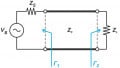
In the previous article in this series, we learned about the effect of mismatch loss on the gain of cascaded amplifiers (Figure 1).
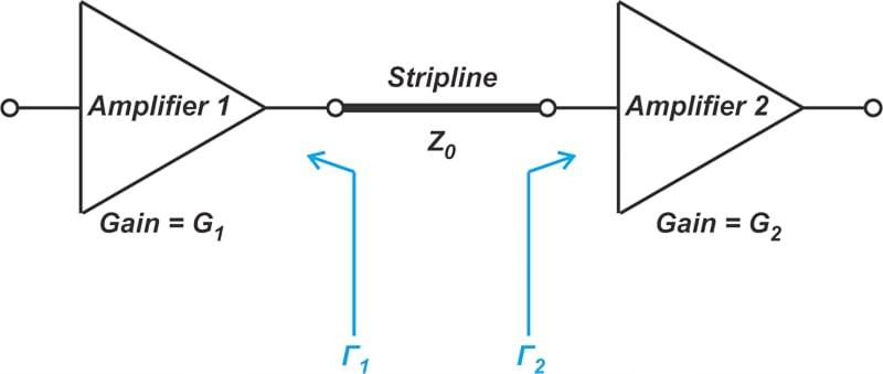
Figure 1. Example diagram showing two amplifiers connected by a stripline.
In this case, the output impedance of Amplifier 1 and the input impedance of Amplifier 2 are not matched with the line’s characteristic impedance. Due to wave reflections, part of the RF energy cannot be delivered to the input of Amplifier 2. The power loss is given in Equation 1:
\[ML= 20log(1 \pm |\Gamma_1||\Gamma_2| )\]
Equation 1.
The above equation corresponds to the case where the transmission line is lossless (gain of 1 or 0 dB). In practice, however, the line exhibits some attenuation.
Accounting for Line Attenuation
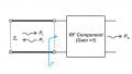
Let’s assume that the magnitude of the line’s voltage attenuation is Ac, where Ac is in linear terms rather than decibels and has a value less than unity. Figure 2 illustrates how a voltage wave traveling in the forward direction (a1) is affected by the line’s attenuation.
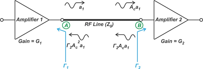
Figure 2. Diagram showing how a voltage wave traveling forward direction is affected by the line's attenuation.
As the signal travels from point A to point B, it gets attenuated by a factor of Ac. Then the signal hits the impedance discontinuity at point B and the reflected signal experiences an additional attenuation of Γ2. At this point, the overall attenuation factor is Γ2Ac. Finally, the signal travels back up the line toward point A with an additional attenuation of Ac. By comparing the incident and reflected signals at point A, the magnitude of the effective reflection coefficient looking from point A into the line is calculated as:
\[|\Gamma_{effective}|=|\Gamma_2| \times A_c^2\]
Equation 2.
Substituting this result in Equation 1, we obtain the mismatch loss for a cable that has an attenuation of Ac:
\[ML= 20log(1 \pm A_c^2 \times |\Gamma_1||\Gamma_2| )\]
Equation 3.
Example 1: Finding Minimum and Maximum Mismatch Loss
Assume that, in a matched environment, the transmission line has a nominal attenuation of 2 dB. If |Γ1| ≤ 0.5 and |Γ2| ≤ 0.33, what are the maximum and minimum of the mismatch-induced loss?
We first need to find the attenuation factor in linear terms:
\[A_c =10^{(-2/20)}=0.794\]
Substituting Ac = 0.794, Γ1 = 0.5, and Γ2 = 0.33 into Equation 3, the maximum and minimum values of ML work out to MLmax = 0.859 dB and MLmin = -0.954 dB. A negative loss of 0.954 dB actually represents a power gain. We can now use these values to find an equivalent loss for the line. We know that the nominal loss of the line is 2 dB. Due to reflections, an additional loss of 0.859 dB or a gain of 0.954 dB is possible. Therefore, the line can have a maximum loss of 2.859 dB or a minimum loss of 1.046 dB.
In addition, we can also say that the maximum gain of the line is -1.046 dB, and the minimum gain of the line is -2.859 dB. If the transducer gain of Amplifiers 1 and 2 are G1 and G2, then the overall gain of the cascade can change between G1 + G2 - 2.859 dB and G1 + G2 - 1.049 dB.
Reducing Mismatch Uncertainty Through Attenuators
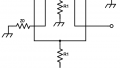
The above discussion leads us to a common solution to reduce the mismatch uncertainty (MU). Comparing Equations 1 and 3, we observe that the line’s attenuation factor effectively reduces the reflection coefficient. Similarly, we can deliberately add a matched, fixed attenuator to suppress the reflected wave. This is shown in Figure 3.
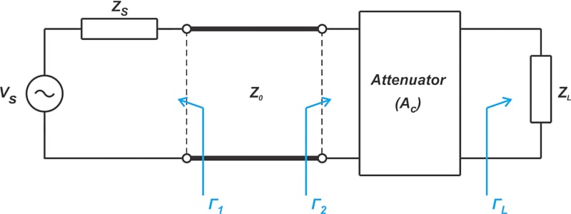
Figure 3. Diagram showing how adding a matched, fixed attenuator can suppress the reflected wave.
The magnitude of the reflection coefficient at the input of the attenuator is:
\[|\Gamma_2| = A_c^2 \times |\Gamma_L|\]
In this case, the MU is:
\[MU = 20log \big ( 1+ A_c^2| \Gamma_1 \Gamma_L| \big ) - 20log \big ( 1 - A_c^2| \Gamma_1 \Gamma_L| \big )\]
If needed, we can also add a fixed attenuator to the input port of the line, as shown below in Figure 4.
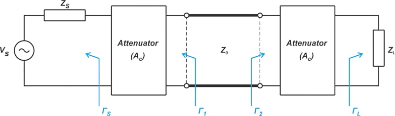
Figure 4. A diagram of a fixed attenuator was added to the line's port.
The reflection coefficient at the input of the line is:
\[|\Gamma_1| = A_c^2 \times |\Gamma_S|\]
Therefore, with both attenuators in place, the MU is:
\[MU = 20log \big ( 1+ A_c^4| \Gamma_S \Gamma_L| \big ) - 20log \big ( 1 - A_c^4| \Gamma_S \Gamma_L| \big )\]
Equation 4.
Example 2: Exploring Mismatch Uncertainty With Attenuators
The reflection coefficient at the input and output of an RF line is 0.3 and 0.4, as shown below.
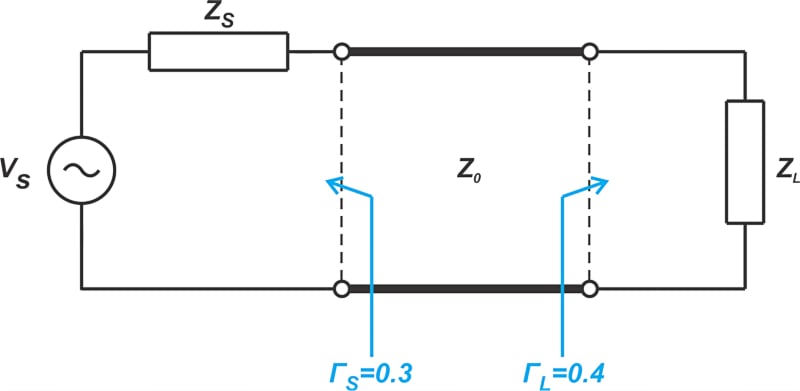
Figure 5. Example diagram showing the input and output of an RF line, ΓS and ΓL.
What is the mismatch uncertainty in this configuration? If we insert two 3-dB attenuators at the input and output of the line, what would be the new mismatch uncertainty?
Without attenuators, we have:
\[\begin{eqnarray}
MU &=& 20log \big ( 1+ | \Gamma_S \Gamma_L| \big ) - 20log \big ( 1 - | \Gamma_S \Gamma_L| \big ) \\
&=& 20 log(1.12)-20log(0.88)=2.094 \text{ } dB
\end{eqnarray}\]
With a 3-dB attenuator, the input-output voltage ratio of the attenuator is:
\[A_c = 10^{-3/20}=0.708\]
Using Equation 4, we find the mismatch uncertainty for the two-attenuator configuration:
\[\begin{eqnarray}
MU &=& 20log \big ( 1+ A_c^4| \Gamma_S \Gamma_L| \big ) - 20log \big ( 1 - A_c^4| \Gamma_S \Gamma_L| \big ) \\
&=& 20 log(1.03)-20log(0.97)=0.52 \text{ } dB
\end{eqnarray}\]
As you can see, the attenuators significantly reduce the mismatch uncertainty.
Masking Pads—Applications and Other Considerations
Attenuators used for mitigating the impedance mismatch are sometimes referred to as “pads,” “masking pads,” or “matching pads.” However, keep in mind that the term "matching pad" is also used for impedance conversion pads that convert between 75 Ω and 50 Ω, and these are different devices.
Masking pads are commonly used in the RF signal path to make the measurements more reliable and predictable. The best place to insert a masking pad is the point where the impedance match is the worst or most variable. One common application of masking pads is RF step attenuators (Figure 6).
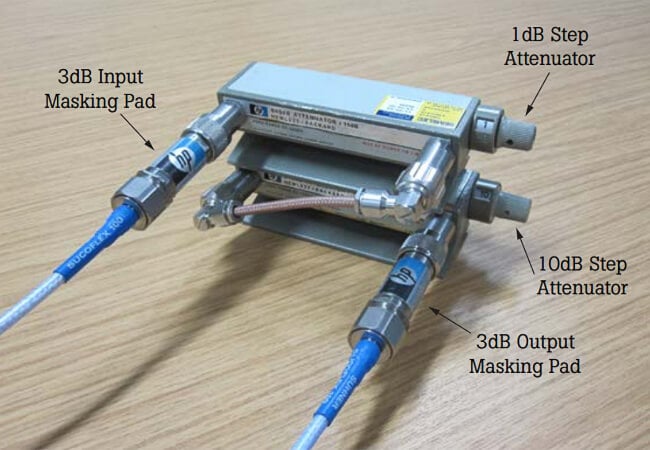
Figure 6. Example application showing the use of masking pads in RF step attenuators. Image used courtesy of Fluke
In the example depicted in the above figure, the step attenuator is fitted with 3-dB masking pads at both the input and output ports to ensure that different settings of the step attenuator exhibit a constant, well-defined match. The main disadvantage of using masking pads is that the attenuator also reduces the amplitude of the desired signal. This can bring the desired signal closer to the noise floor. For example, with a single 3 dB attenuator, the return loss of a given load ideally improves by 6 dB; however, the amplitude of the forward traveling wave is also reduced by 3 dB.
It is also possible to use a matching network to achieve the required impedance match without significantly attenuating the desired signal. However, one major advantage of a masking pad over a matching network is that masking pads can provide a flat frequency response across the specified frequency range. For example, a low-valued attenuator might have an attenuation variation of ±0.2 dB over the DC to 18 GHz frequency range. This is not the case for impedance-matching networks that normally provide the impedance match over a narrow frequency range.
Mismatch Uncertainty Plot
It is instructive to examine how mismatch uncertainty changes as a function of Γ1 and Γ2. This is shown in Figure 7, which is taken from this Keysight application note.
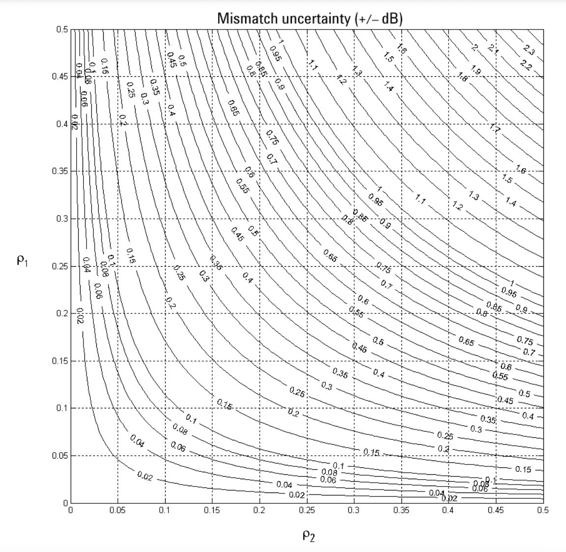
Figure 7. A plot showing mismatch uncertainty changes. Image used courtesy of Keysight [click image to enlarge]
The plots show the variation of MU in ±dB. For example, with Γ1 = Γ2 = 0.05, we know that the mismatch uncertainty is about ±0.021 dB, which is consistent with the above set of plots. The important observation here is that by making one of the reflection coefficients sufficiently low, we can control the mismatch uncertainty. For example, with Γ1 = 0.05 (corresponding to a VSWR of 1.1), the mismatch uncertainty remains below about ±0.2 dB even when Γ2 = 0.5 (or VSWR is 3). As an example, consider the RF power measurement application. If you choose a power sensor with low VSWR, you can ensure that you have somewhat controlled the mismatch uncertainty based on how low the VSWR of your sensor is (and regardless of the VSWR of the power source).
Statistical Models of Mismatch Uncertainty
In the above discussion, we only considered the upper and lower bounds of the mismatch uncertainty. While this gives us a sense of the worst-case uncertainty in the circuit, it is useful to have a statistical model of the error. The Keysight application note I mentioned above summarizes different probability density functions (PDF) that can be considered for the mismatch uncertainty. To find the PDF of MU, three different distributions are considered for Γ1 and Γ2, as shown in Figure 8.
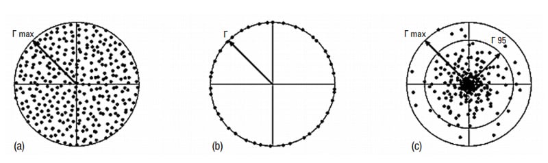
Figure 8. Examples showing three different distributions for Γ1 and Γ2. Image used courtesy of Keysight.
Combining these distributions, six different PDF functions are found for the mismatch uncertainty. For example, assuming that both Γ1 and Γ2 have ring distributions (Figure 8(b)), MU has the well-known U-shaped distribution, as shown in Figure 9.

Figure 9. Example chart showing how the MU has a U-shaped distribution. Image used courtesy of Keysight [click image to enlarge]
These statistical models allow us to estimate the standard deviation of the mismatch uncertainty. For more information, please refer to the Keysight document linked earlier in this article.
RF Design and Mismatch Uncertainty
Mismatch uncertainty is an important factor to consider when designing a cascade of RF blocks or making RF measurements. One common method of reducing the mismatch uncertainty is to place a matched attenuator in front of a mismatched impedance. When dealing with this error, we are interested in finding the upper and lower bound of the error and its PDF function so that we can estimate the standard deviation of the error.
To see a complete list of my articles, please visit this page.