
RF Design Basics: VSWR, Return Loss, and Mismatch Loss
Learn about voltage standing wave ratio (VSWR), return loss, and mismatch loss, which helps characterize the wave reflections in a radio frequency (RF) design.
Electrical waves reflect when they encounter a change in the impedance of the medium they are traveling in. These reflections are very undesirable when we aim to transfer power from one block to the next one in the signal chain.
In this article, we’ll learn about two parameters, namely VSWR and return loss, that allows us to characterize wave reflections in an RF design. We’ll also discuss the “mismatch loss” specification that parameterizes the effect of wave reflections on power transfer.
Calculating the VSWR Formula
With a short-circuited or open-circuited transmission line, total reflection occurs, and the interference of the incident and reflected waves creates standing waves on the transmission line. As an example, consider the diagram shown in Figure 1.
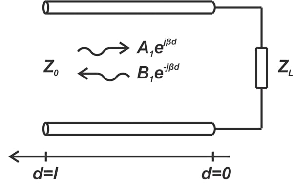
Figure 1. Example diagram.
For a sinusoidal input, the steady-state response is also sinusoidal. With a length of d = 0.2 meters and a short-circuited load (ZL = 0), the voltage wave along the line at 36 different instants is shown in Figure 2.
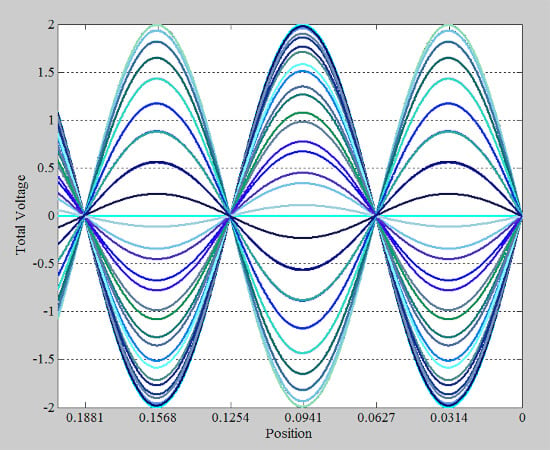
Figure 2. Voltage waves at 36 different instances.
The above curve gives you a sense of how the amplitude of the voltage wave changes along the line. This amplitude variation is best shown by the envelope of the above plots, provided in Figure 3 below.
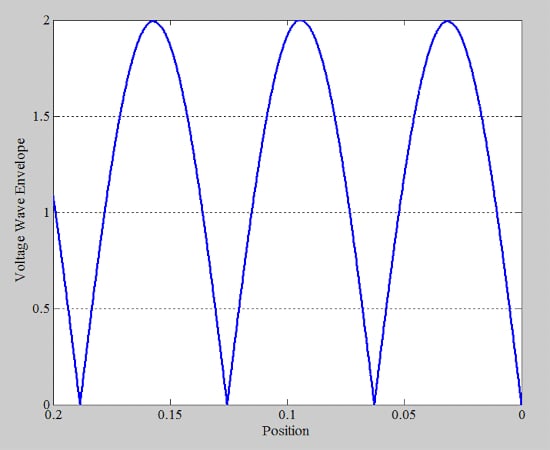
Figure 3. Amplitude variation plot.
Note that the minimum value of the envelope is zero volts. We can repeat the same procedure for an arbitrary load, say a load with Γ = 0.5. The voltage wave plots for this case at 36 different instants are shown in Figure 4.
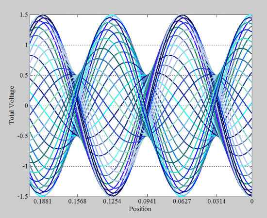
Figure 4. Another example plot shows the voltage wave for 36 instances.
The envelope of these curves is shown in Figure 5.
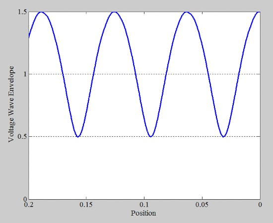
Figure 5. Example voltage wave envelope vs. position plot.
The above discussion shows that when total reflection occurs, the minimum value of the envelope is zero volts Vmin = 0 (Figure 3). With partial reflection, however, Vmin gets closer to the peak value Vmax. In the ideal case where there is no reflection, Vmax becomes actually equal to Vmin. Therefore, the ratio of Vmax to Vmin, known as the VSWR, is related to the amount of reflection that occurs at the impedance discontinuity. In mathematical language, VSWR is defined as:
\[VSWR = \frac{V_{max}}{V_{min}}\]
Equation 1.
When there’s total reflection, VSWR is infinite; for a matched load, VSWR is 1; and for other cases, VSWR is between these two extreme values. As an example, for the envelope waveform in Figure 5, VSWR is:
\[VSWR = \frac{V_{max}}{V_{min}}=\frac{1.5}{0.5}=3\]
It can be easily shown that VSWR is related to the load reflection coefficient Γ by the following equation:
\[VSWR = \frac{1+| \Gamma |}{1-|\Gamma|}\]
Equation 2.
This equation allows us to measure VSWR and use that information to determine the magnitude of the reflection coefficient.
As a side note, the VSWR parameter might somewhat have lost the significance it once had. Today’s high-performance directional couplers can separate the incident and reflected waves physically, enabling us to accurately measure the reflection coefficient.
In the early years of transmission line measurements, these high-performance directional couplers were unavailable, and Equation 2 served as an easy solution to measure the magnitude of Γ. To this end, engineers only needed to measure the minimum and maximum voltages along the line through a device called a slotted line. Considering the availability of today’s high-performance measurement equipment, VSWR is sometimes considered a left-over parameter from decades ago. However, RF engineers need to fully understand the VSWR concept as it is still commonly specified in datasheets.
RF Return Loss
Consider the diagram in Figure 6, where a transmission line is connected to the input of an RF component. The incident power is Pi, and the reflection coefficient “looking” into the RF component’s input is Γ.
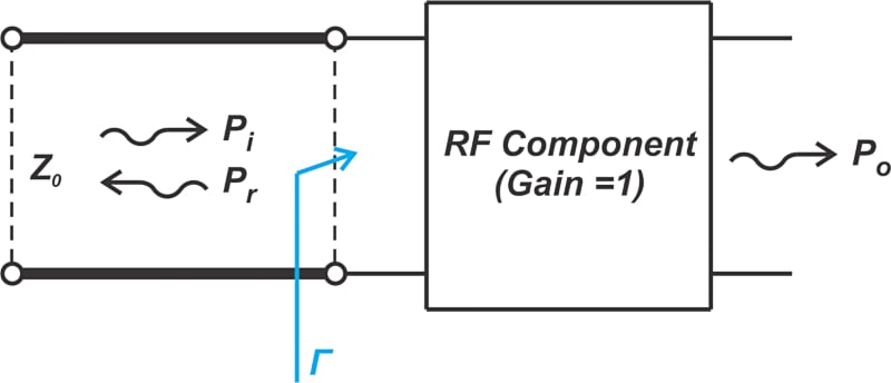
Figure 6. Diagram showing the RF component and transmission line.
Here, we are interested in characterizing how much of the incident power is reflected from the RF component (Pr). While the reflection coefficient Γ is the ratio of the reflected voltage to the incident voltage, \(|\Gamma|^2\) represents the ratio of the reflected power to the incident power:
\[P_r = |\Gamma|^2 P_i\]
Equation 3.
Expressing the above equation in decibels produces:
\[P_r|_{dB} = P_i |_{dB}+10log(|\Gamma|^2)\]
Equation 4.
For example, if \(|\Gamma|^2=0.1\), we get:
\[P_r|_{dB} = P_i |_{dB}-10 dB\]
This means that the reflected power is 10 dB lower than the incident power. In this case, we can say that the part of the incident signal that returns experiences a gain of -10 dB or, equivalently, a loss of +10 dB. In other words, the “return loss” is 10 dB in this example.
Alternatively, the return loss parameter is commonly used to express Equations 3 and 4. The name of this parameter, however, might be a bit confusing at first. Return loss specifies the loss that the incident signal experiences as it returns or reflects from the impedance discontinuity.
Note that for passive circuits, Γ is bounded between 0 and 1, and therefore, the signal that returns experiences an attenuation or loss rather than a gain. Return loss, commonly denoted by RL, is given by:
\[RL=-20 log(|\Gamma|)\]
Equation 6.
For example, if the return loss in a system is specified to be 40 dB, you instantly know that the reflected power is 40 dB lower than the incident power. Therefore, a larger return loss corresponds to a better match between the load and the line’s characteristic impedance.
The three parameters Γ, VSWR, and return loss are all different ways of specifying how well the load is matched to the transmission line. However, unlike Γ, which has both magnitude and phase information, VSWR and return loss provide magnitude only and don’t have phase information.
Mismatch Loss
Let’s examine the configuration in Figure 6 one more time. In addition to the reflected power, we’re also interested in characterizing the effect of impedance mismatch on the amount of power that gets transferred to the output Po. First, assume that the power gain of the RF component is unity (G = 1). In other words, the same power that is delivered to the input of the RF component appears at its output. Since impedance mismatch leads to some reflected power, it reduces the power that is passed on to the RF component. With G = 1, the output power Po is equal to the difference between the incident power and the reflected power:
\[P_o = P_i - P_r =P_i (1- |\Gamma|^2)\]
Expressing the above equation in decibels leads to:
\[P_o|_{dB} = P_i|_{dB}+10log \Big (1- |\Gamma|^2 \Big)\]
Continuing with the example value of \(|\Gamma|^2=0.1\), the above equation produces:
\[P_o|_{dB} = P_i|_{dB}+10log (0.9)=P_i|_{dB}-0.46 \text{ } dB\]
This means that the output power is 0.46 dB lower than the incident power. In other words, the signal experiences a gain of -0.46 dB or, equivalently, a loss of +0.46 dB. This loss of power is referred to as the “mismatch loss” because it originates simply from the impedance mismatch. The mismatch loss parameter tells us how much gain improvement we can get by providing a perfect impedance match. In the above example, the obtainable gain improvement is 0.46 dB. Based on the above discussion, the mismatch loss, denoted by ML, is given by the following equation:
\[ML=-10log \Big (1- |\Gamma|^2 \Big)\]
Equation 7.
From the above explanation, it should be clear that a small mismatch loss is desired and corresponds to a better match between the load and line.
Mismatch Loss When Both Ports are Mismatched
In Figure 6, we implicitly assumed that the impedance of the signal source (not shown) is matched to the line characteristic impedance. If this is not the case, Pr will re-reflect off the discontinuity at the source end and contribute to the incident wave Pi. This situation is encountered, for example, when we connect a source to a load through a transmission line (Figure 7(a)) as well as at the interface between two cascaded devices (Figure 7(b)).
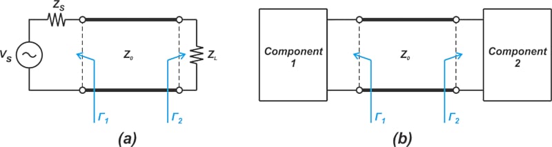
Figure 7. Example diagram of a source connected to a load through a transmission line (a) and the interface between two cascaded devices (b).
In this case, the mismatch loss (in linear terms rather than decibels) is given by Equation 8.
\[ML = \frac{|1- \Gamma_1 \Gamma_2|^2}{\big ( 1-|\Gamma_1|^2 \big )\big ( 1-|\Gamma_2|^2 \big )}\]
Equation 8.
The above equation specifies the portion of the input power that bounces back and forth between the input and output ports due to wave reflections. You can find the derivation of this equation in Chapter 2 of “Microwave Transistor Amplifiers” by G. Gonzalez. For example, assume that Γ1 and Γ2 are respectively 0.1 and 0.2 in Figure 7(a). In this case, we have a mismatch loss of ML = 1.011. Expressed in dB, we have a loss of 0.05 dB because of the two impedance discontinuities.
Note that Γ has both magnitude and phase information, and the phase angle can affect the ML value produced by Equation 8. Let’s repeat the above example with Γ1 = 0.1 and Γ2 = -0.2. In this case, ML works out to 1.095 or 0.39 dB.
Mismatch Uncertainty
The above example highlights a serious challenge in RF applications. Since mismatch loss in Equation 8 depends on the phase angle of the reflection coefficients and noting that in many practical situations, only the magnitude of the reflection coefficient is known, there is some uncertainty about how much power is actually transferred from the input to the output. For example, knowing that |Γ1| = 0.1 and |Γ2| = 0.2, the mismatch loss is somewhere between 0.05 dB and 0.39 dB. The range specified by these upper and lower bounds is called the mismatch uncertainty, which we’ll look at in greater detail in the next article in this series.
Featured image used courtesy of Adobe Stock
To see a complete list of my articles, please visit this page.


Nice intro to the formulas dealing with impedances and miss match.
However you have so much wrong in your presentation.
A 40dB feed with a 40dB VSWR ? A perfect feed? That would be a total cancelation of the signal. A perfect miss match.
As a former radio engineer, I know of what I speak.
You need to match the output of your transmitter to the feed line. And then to the actual transmitting device, such as your broadcast tower.
With short feed lines, you may get by with a tuning unit just at the antenna.
Sorry, but I have a problem with people that are all theory and no real world.
Excellent presentation. Thank you!