Facebook
 Google
 GitHub
 Linkedin
Mismatch Loss and Mismatch Uncertainty in RF Systems
Learn more about RF wave reflection parameters, namely mismatch loss and mismatch uncertainty.
Signal reflection is a commonly encountered phenomenon in RF systems and can reduce the power that reaches a load. When designing a cascade of RF blocks, wave reflections can lead to uncertainty about how much power gain the cascade will exhibit in the final design. To better understand this, let's go over mismatch loss (ML), which is the parameter that characterizes the power loss caused by wave reflections.
Mismatch Loss Formula
When both the input and output ports of a transmission line are connected to mismatched impedances (Zs ≠ Z0 and ZL ≠ Z0), a portion of the power provided by the input bounces back and forth between the input and output ports (Figure 1).
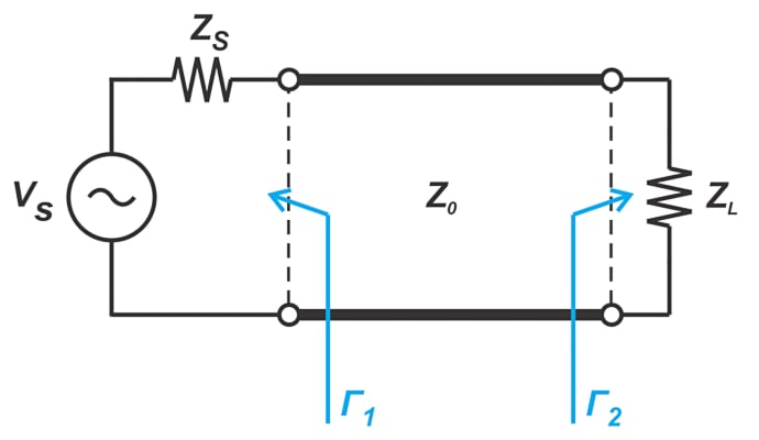
Figure 1. Example showing the transmission line's input and output ports connected by mismatched impedances.
Such wave reflections lead to a loss of power that is characterized by the ML parameter, shown in Equation 1.
\[ML = \frac{|1- \Gamma_1 \Gamma_2|^2}{\big ( 1-|\Gamma_1|^2 \big )\big ( 1-|\Gamma_2|^2 \big )}\]
Equation 1.
In many applications, the phase angle of Γ1 and Γ2 is unknown. In these cases, we can only find the upper and lower bound of ML to determine the range of power transfer uncertainty. Equations 2 and 3, respectively, show the upper and lower limits of ML.
\[ML_{max} = \frac{|1+ | \Gamma_1 \Gamma_2||^2}{\big ( 1-|\Gamma_1|^2 \big )\big ( 1-|\Gamma_2|^2 \big )}\]
Equation 2.
\[ML_{min} = \frac{|1- | \Gamma_1 \Gamma_2||^2}{\big ( 1-|\Gamma_1|^2 \big )\big ( 1-|\Gamma_2|^2 \big )}\]
Equation 3.
Expressing these two last equations in decibels and finding the difference yields the uncertainty range, shown in Equation 4.
\[MU = 20log \big ( 1+ | \Gamma_1 \Gamma_2| \big )- 20log \big ( 1 - | \Gamma_1 \Gamma_2| \big )\]
Equation 4.
This uncertainty range is known as mismatch uncertainty (MU) in the RF literature.
Mismatch Loss and Uncertainty Example 1: Examining the Transmission Line Effect
To better understand the above concepts, we use LTspice to simulate the circuit in Figure 1 with parameters ZS = ZL = 50 Ω and Z0 = 75 Ω. The LTspice schematic is shown in Figure 2.
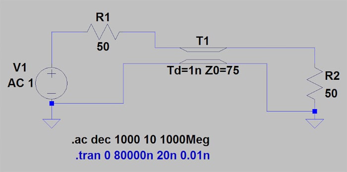
Figure 2. Example LTspice schematic.
The transmission line has a propagation delay of 1 ns. This is a convenient method for expressing the physical length of a transmission line: the amount of time it takes a wave to propagate down the length of the line. Next, we sweep the frequency of the AC source from 10 Hz to 1 GHz to find the load voltage and current. Using this information, we can find the power dissipated in the load whose plot is provided in Figure 3.
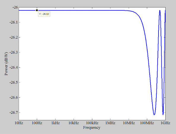
Figure 3. Example plot showing the power dissipated in the load.
At low frequencies, for example, those below 10 MHz, the transmission line effect is negligible as if the load is directly connected to the signal source. In this case, half of the input voltage appears across the load (VLoad = 0.5 V), and the power delivered to the load is found as:
\[P_{Load}=\frac{V_{Load}^2}{2Z_{L}}=2.5 \text{ }mW=-26.02 \text{ }dBW\]
This is consistent with the above plot. As we increase the frequency, the transmission line effect manifests itself. Additionally, the phase angle of the reflection coefficient (at a fixed distance from the impedance discontinuity) varies linearly with the input frequency. Therefore, from Equation 1, we expect the dissipated power to change with frequency. This is best illustrated by plotting the power curve using a linear x-axis, as shown in Figure 4.
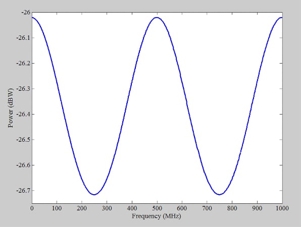
Figure 4. Example plot showing the power curve using a linear x-axis.
As the input frequency changes, the dissipated power rises and falls in a cyclic fashion. The first maximum of the curve occurs at 500 MHz. You might wonder: why do we have a maximum at 500 MHz?
The round-trip time for the incident wave to reach the line’s end and reflect back to the source is 2 ns in our example. On the other hand, the period of a 500 MHz signal is also 2 ns. Therefore, with a 500 MHz signal, the reflected wave adds in phase with the incident wave, maximizing the power transfer.
Note that the phase angle of the reflection coefficients should also be considered in this intuitive explanation. However, in our example, the reflection coefficients are negative real values (Γ1 = Γ2 = -0.2) that enable constructive interference at 500 MHz.
With that in mind, how are Equation 1 and its limits related to the curve in Figure 4? The MU (Equation 4) is the difference between the upper and lower bounds of the ML. Thus, it gives us the total variation in the load power. If we substitute Γ1 = Γ2 = -0.2 into Equation 4, the mismatch uncertainty works out to MU = 0.7 dB. This is consistent with the peak-to-peak variation of the power curve in Figure 4.
The Reference Power is Important for Mismatch Loss
We discussed above that Equation 1 characterizes the power loss caused by impedance discontinuities. This description doesn’t provide an important piece of information: the reference (or maximum power) that we expect the system to deliver to the load when there is no mismatch-induced power loss (ML = 1 or 0 dB). In other words, we don’t know the reference power the loss term is calculated. If you go through the derivation of Equation 1, you’ll notice that the reference power is the power available from the source PAVS. The power available from the source is the power delivered by the source to a conjugately matched load. This occurs when Γ2 = Γ1*, where the * denotes the complex conjugate operation. With ML expressed in linear terms (rather than decibels), the relationship between PAVS and the delivered power PLoad is given via Equation 5.
\[P_{Load}=\frac{P_{AVS}}{ML}\]
Equation 5.
Note that with Γ2 = Γ1*, Equation 1 yields ML = 1. This means that when the load is conjugately matched, the loss term vanishes ML = 1 (or 0 dB). To better understand these concepts, let’s examine another LTspice simulation.
Mismatch Loss and Uncertainty Example 2: Using AC Analysis
Consider the following diagram in Figure 5.
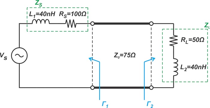
Figure 5. An example diagram where the source and load impedances have real and imaginary parts to them.
In this case, the source and load impedances have both real and imaginary parts. We can use an AC analysis to sweep the input frequency and observe the changes in the dissipated power. However, we’ll use another (actually more interesting) method in this example: we’ll keep the input frequency constant while sweeping the delay of the transmission line through a range of values. At 198.943 MHz, a 40 nH inductor has an impedance of j50 Ω. We’ll examine the circuit at this frequency simply because it produces some easy numbers to work with. The LTspice schematic is shown in Figure 6.
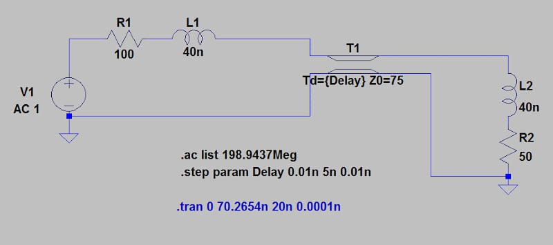
Figure 6. LTspice schematic for the example in Figure 5.
Note that the transmission line delay is defined as a parameter (‘Delay’). Using the .step command, the ‘Delay’ parameter is linearly swept from 0.01 ns to 5 ns with steps of 0.01 ns. Also, using the ‘list’ option, the AC Analysis is performed only at a single frequency (198.943 MHz). The amplitude of the AC input is 1 V, as is common in AC simulations. This simulation gives us the load voltage and current. Using that information, we can find the average power delivered to the load, as shown by the blue curve below (Figure 7).
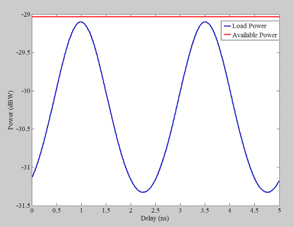
Figure 7. Plot showing the average power delivered to the load.
Also, we can use a logarithmic scale for the x-axis to better observe the circuit response for very small values of delay. This is shown in Figure 8.
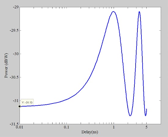
Figure 8. Plot using a logarithmic scale for the x-axis for circuit response.
Let’s now use our equations to verify the above curves. Before that, we need to find our equivalent circuit at the frequency of interest (198.943 MHz). At this frequency, a 40 nH inductor has an impedance of j50 Ω, leading to the following diagram of Figure 9.
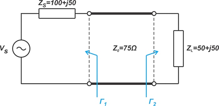
Figure 9. Example diagram for an equivalent circuit with a frequency of interest (198.943 MHz).
The first question is: why does the load power change as a function of the line’s delay? As can be seen from Equation 6 below, the load reflection coefficient at the load end of the line (Γ2) is constant at a given frequency:
\[\Gamma_2 = \frac{Z_L - Z_0}{Z_L + Z_0}=\frac{(50+j50)-75}{(50+j50)+75}=0.415\angle 94.76^\circ\]
Equation 6.
However, even with a lossless line, the phase angle of the reflection coefficient changes along the line. This change in phase angle determines whether the incident and reflected waves will interfere constructively or destructively at the source end of the line. By sweeping the transmission line’s delay, the phase angle of the reflection coefficient and, consequently, the power delivered to the load is changed.
The next question: how much power is transferred at very small values of delay where the transmission line effect is negligible? Figure 8 shows that for delays less than about 0.03 ns, the load power is almost constant. In this range of delays, the transmission line effect is almost negligible as if the load is directly connected to the source (Figure 10).
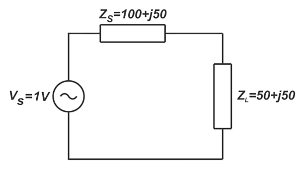
Figure 10. Diagram showing the load directly connected to the source.
Using basic circuit theory concepts, you can verify that the average power that the above circuit delivers to the load is 0.77 mW or -31.13 dBW. This is consistent with Figure 8. What is the maximum power that the source can deliver to a conjugate-matched load? With a source impedance of ZS = 100+j50, the power available from a 1 V source is found using Equation 7.
\[P_{AVS}=\frac{V^2}{8R_S}=\frac{1^2}{8 \times 100}=1.25\text{ } mW=-29.03 \text{ }dBW\]
Equation 7.
This is the maximum power that the source can provide to a conjugate-matched load. In our circuit, the load is not the conjugate of the source impedance, and thus, the dissipated power is always lower than PAVS (the red curve in Figure 7). Using Equations 2 and 3, we can find the limits of mismatch loss. We first need to find Γ1 using Equation 8.
\[\Gamma_1 = \frac{Z_S - Z_0}{Z_S + Z_0}=\frac{(100+j50)-75}{(100+j50)+75}=0.307\angle47.49^\circ\]
Equation 8.
Substituting Γ1 and Γ2 into Equations 2 and 3 yields MLmin = 0.07 dB and MLmax = 2.29 dB. Subtracting these values from the available power (-29.03 dBW) gives us the maximum and minimum values of the delivered power PL, max = -29.1 dBW, and PL,min = -31.32 dBW. These values are also consistent with the maximum and minimum of the power curve in Figure 7.
The Mismatch Loss Equation and Power Loss
The mismatch loss equation allows us to characterize how much of the source power is lost because of wave reflections at the input and output ports of a transmission line. By investigating two examples, we tried to show the subtleties of the mismatch loss equation. The equation discussed in this article gives the power loss with respect to the power available from the source. It should be noted that there is another commonly used mismatch loss equation whose reference power is the power that the source can deliver to a Z0-terminated load rather than a conjugate-matched load. This will be discussed in the next article.
To see a complete list of my articles, please visit this page.