 Facebook
 Google
 GitHub
 Linkedin
Why Do We Need Matched Termination with High Speed Logic Families?
This article will try to develop a better insight into wave reflection that can occur when driving a relatively long wire with a fast logic gate.
This article will try to develop a better insight into wave reflection that can occur when driving a relatively long wire with a fast logic gate.
Related Information
Delay of Wires
An electrical signal has a finite speed when travelling through a wire. The exact value of the speed depends on the characteristics of the wire, but we can assume a speed of about half the speed of light, which is nearly $$\tfrac{1}{2} \times 3 \times 10^8$$ m/s. Therefore, an electrical signal needs about 1 nanosecond (ns) to propagate through a 15 centimeter (cm) wire.
The Signal Rise and Fall Time
Now, assume that we have a fast logic family which exhibits rise and fall times of about 1 ns. What happens if we connect this high speed logic to a relatively long wire that introduces a delay comparable to the signal rise time?
As you may have guessed, in such cases, we may not be able to treat the wire as an ideal zero-delay conductor. In fact, the logic gate may apply a voltage transition to the beginning of the wire while the other end of the wire still has its previous voltage value. Can this phenomenon give us trouble? We’ll answer this question later in the article. First we’ll discuss transmission lines.
Transmission Lines
When we’re working with high-speed signals, we often need to think in terms of transmission lines instead of ordinary wires. Transmission lines require special analysis techniques, and they are implemented with greater attention to such details as the distance between a conductor and a ground shield or the dimensions of a PCB trace. A transmission line can be modeled as follows:
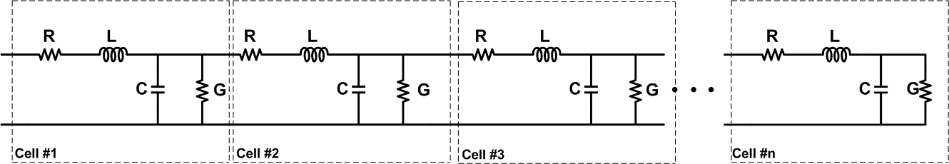
Figure 1. Click to enlarge.
The transmission line is divided into smaller sections, and each section is modeled using some passive elements. As shown in the figure, these passive components are distributed along the wire. Here, R and G represent, respectively, the resistance of the wire and the conductance of the dielectric that separates the conductors. L and C represent the inductance and the capacitance of the transmission line.
Note that generally the distributed element model for a transmission line uses an infinite series of cells as shown in Figure 2 below.
![]()
Figure 2. Cell schematic used to model a transmission line. Image courtesy of Omegatron [CC BY-SA 3.0]
In Figure 2, the value of the components R, L, G, and C are specified per unit length. However, in our model shown in Figure 1, the value of the components are not per unit length. In Figure 1, we assume that a given length of the transmission line is divided into sufficiently small segments (or, equivalently, n is sufficiently large), so that each segment can be represented by some passive components. Using this model, we'll provide an intuitive understanding of the electrical wave reflection in a transmission line. To simplify this article’s discussion, we'll assume that the wire is lossless (R = G = 0). This will give the model shown in Figure 3.
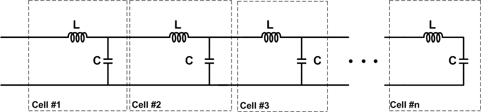
Figure 3. Click to enlarge.
As mentioned above, we intend to develop an intuitive understanding of the reflection phenomenon based on the circuit model of a lossless transmission line. While the overall shape of the waveforms given below can be verified by circuit simulations, there can be differences between the waveforms obtained from a circuit simulator (examples are given at the end of the article) and the simplified plots provided in the more theoretical discussion of this topic. However, the main goal of this article is not discussing the exact waveforms; instead, we want to explain electrical wave reflection by replacing a transmission line with its circuit model.
Now, let’s use the model in Figure 3 to examine connecting a high-speed logic gate to a wire that is long with respect to the signal rise time.
A Transmission Line of Infinite Length
First, assume that the gate is connected to a transmission line of infinite length. Figure 4 shows a model for the low-to-high transition. In this figure, Rs is the output impedance of the gate when going from logic low to logic high and Vs is the logic-high voltage. In this article, we’ll assume that the output resistance of the gate, Rs, is equal to $$\sqrt{ \tfrac{L}{C} }$$. The reason for this assumption will be explained at the end of the article.
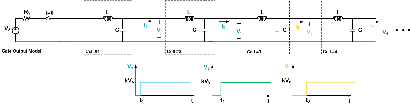
Figure 4. Click to enlarge.
In Figure 4, we have assumed a very abrupt transition from low to high. The figure shows that the cells that are farther along the wire experience a larger delay, i.e., $$t_3$$ > $$t_2$$ > $$t_1$$. Also, note that while the input source applies a transition from 0 to Vs, the voltage transitions of the cells are from zero to kVs! The factor k is less than one; we won’t go through the mathematics needed to derive the exact value.
We have assumed that the line is of infinite length. Thus, there is always a cell along the wire that hasn’t experienced the voltage transition yet. The current that causes the transition for this particular cell must be supplied by the voltage source placed at the beginning of the wire. This current will have to flow through the cells that are closer to the source, and eventually it will be delivered to the cell experiencing the voltage transition. Since the current is flowing from the source toward the wire, we can conclude that the voltage developed across the cells is less than Vs(i.e., k<1).
It can be shown that the factor k is equal to $$\tfrac{Z_0}{Z_0+R_S}$$, where $$Z_0$$ is the characteristic impedance of the transmission line. The characteristic impedance is determined by the geometry and materials of the transmission line and, for a uniform line, is not dependent on its length. Refer to the textbook page on transmission lines in the AAC RF textbook for more details.
A Short-Circuited Transmission Line
Now that we’re familiar with an electrical wave propagating through a wire of infinite length, let’s examine the propagation along a short-circuited transmission line, as shown in Figure 5. To simplify our discussion, we are showing only four cells in the figure.
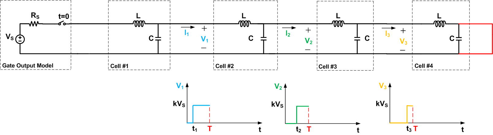
Figure 5. Click to enlarge.
The figure presents the waveforms for $$t < T$$, where T is the delay from the beginning of the transmission line to its far end, which is short-circuited by the red wire. For $$t < T$$, the waveforms of Figure 5 and 4 are the same. In fact, in this interval, the short-circuit forces zero voltage across the fourth cell of Figure 5 but note that this voltage was initially assumed to be zero in Figure 4.
However, for $$t > T$$, the two circuits exhibit different behavior. In Figure 5, the output of the fourth cell is forced to remain at zero volts. The short circuit actually provides a path for discharging the previous cells too. That’s why after some delay $$V_3$$ will exhibit a transition to zero. This will in turn cause $$V_2$$ to go to zero after some delay. Hence, we obtain the final waveforms as shown in Figure 6.
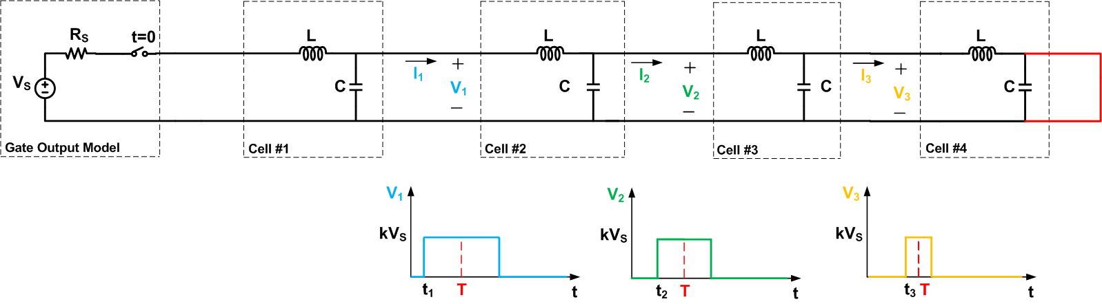
Figure 6. Click to enlarge.
An Open-Circuited Transmission Line
Now, let’s examine the electrical wave propagation along an open-circuited transmission line as shown in Figure 7. Again, to simplify our discussion, we are showing only four cells in the figure.
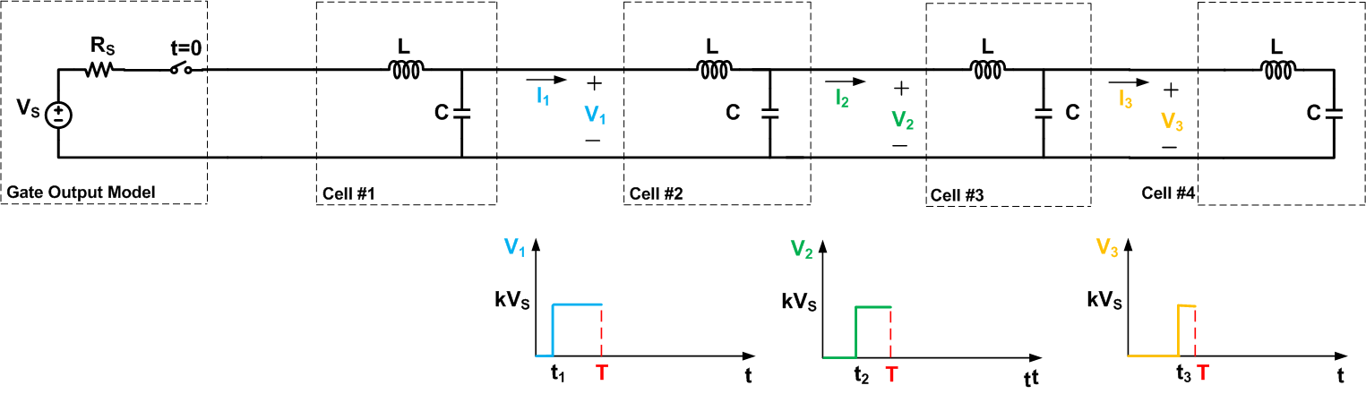
Figure 7. Click to enlarge.
The figure also depicts the waveforms for t
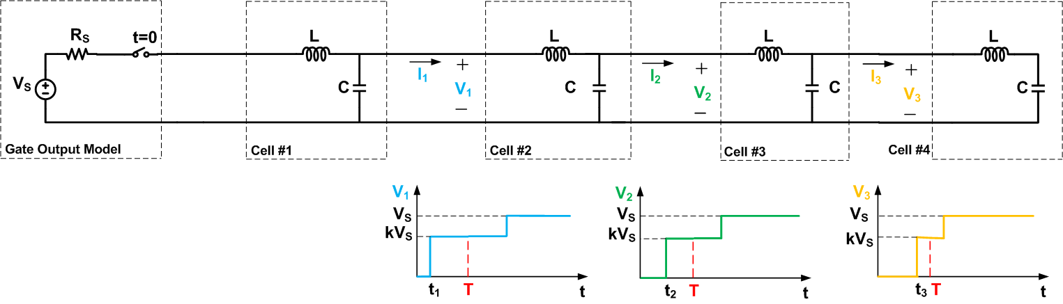
Figure 8. Click to enlarge.
Reflection Coefficient
To have a unified treatment of the problem, we can define a reflection coefficient:
$$\rho = \frac{Z_{term}-Z_0}{Z_{term}+Z_0}$$
Where $$Z_{term}$$ and $$Z_0$$ are the termination impedance and the characteristic impedance of the transmission line. For example, consider the waveforms shown in Figure 6. In this case, the termination impedance is zero which gives $$\rho =-1$$. This means that the original waveform shown in Figure 5 will be reflected with a reflection coefficient of -1. In other words, a wave with magnitude equal to the original wave but with the opposite polarity will be reflected from the short-circuited end of the transmission line.
For the waveforms of Figure 8, the terminating impedance is infinity which gives $$\rho=1$$. Hence, a wave equal to the original wave will be reflected from the open-circuited end of the transmission line. Adding the reflected waveform to the original waveform leads to the waveforms shown in Figure 8.
Avoiding Reflections
The above discussion shows the importance of the resistance that terminates a transmission line. As you can see from the examples, different termination resistances lead to different reflection coefficients. How can we avoid reflections?
We observed that there’s no reflection when the transmission line is of infinite length. In practice, we cannot have a transmission line with infinite length, but we can use a termination resistance equal to the characteristic impedance of the line to avoid reflections. This can be also verified using Equation 1 which gives $$\rho=0$$ for $$Z_{term}=Z_0$$. For example, when positive-referenced emitter-coupled logic (PECL) is driving a load through a transmission line, we terminate the transmission line to a resistance close to the characteristic impedance of the line. This is shown in Figure 9.
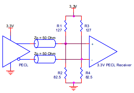
Figure 9. Thevenin termination for a PECL gate driving a 50 transmission line. Image courtesy of idt.
In the example of Figure 9, the termination resistance is $$R_1 || R_2 =50 \Omega $$ which is equal to the characteristic impedance of the line. It’s worthwhile to note that, in addition to providing a matched termination, the values of the resistors determine the DC level for the input of the PECL receiver. In this example, the resistors are chosen to set the DC level of the inputs to about 1.3V.
In the above examples, we saw that the end of the transmission line can reflect the propagating wave when $$Z_{term}$$ is not equal to $$Z_0$$. It should be noted that the reflected wave itself can be re-reflected when reaching the beginning of the transmission line if the source resistance, Rs, is not equal to $$Z_0$$. Since the characteristic impedance of a lossless transmission line is equal to $$\sqrt{\tfrac{L}{C}}$$, we assumed $$Rs=\sqrt{\tfrac{L}{C}}$$ at the beginning of the article to avoid re-reflection of the reflected waves.
If the rise time of the logic gate is longer than 2T, where T is the delay of the wire, then we can ignore the reflections. In this case, the reflections return while the input is still rising, so we’ll have a somewhat slowed and “bumpy” rising edge but the overall functionality will be fine.
Some Simulations
In previous sections, we used a circuit model to examine electrical wave reflection along a transmission line. Now, we’ll look at some waveforms obtained from circuit simulations. In these simulations, we have cascaded 20 LC cells to model a hypothetical transmission line. Similar to the schematic shown in Figure 5, the end of the transmission line is short-circuited. A low to high transition is applied to the beginning of this transmission line. In the first simulation waveform shown in Figure 10, we have chosen L = 2.5 nH and C = 1 pF. In this figure, the red curve is the pulse applied to the input of the transmission line and the blue curve is the voltage observed at the output of the 10th cell. As you can see, at first, we have a transition from low to high. Then, after some delay, the waveforms exhibit a transition from high back to low. This is consistent with the waveforms we obtained for Figure 5. However, unlike the waveforms of Figure 5, we have some ringing behavior in Figure 10.
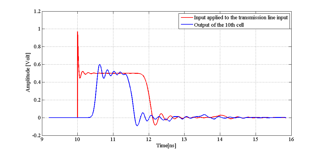
Figure 11. Simulation waveforms for a short-circuited transmission line model with L = 2.5 nH and C = 1 pF. Click to enlarge.
Now, we will change the value of L and C to 0.05 nH and 0.02 pF. In this case, the waveforms are as shown in Figure 11.
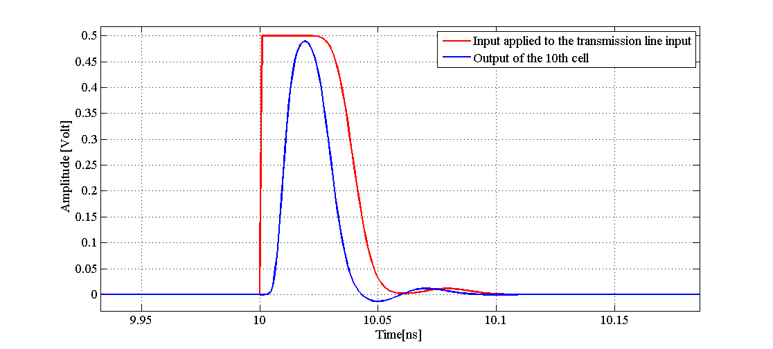
Figure 11. Simulation waveforms for a short-circuited transmission line model with L = 0.05 nH and C = 0.02 pF. Click to enlarge.
Comparing Figure 10 with Figure 11, we observe that there may or may not be ringing effect but the overall behavior is as discussed in the article: with a short-circuited line at the far end, the voltage waveforms return to zero volts due to the wave reflection phenomenon. Why do you think the value of L and C can affect the ringing behavior of the waveforms? If you have any explanation for this phenomenon, feel free to share it with us in the comments below.
To see a complete list of my articles, please visit this page.


While I agree about the statement: “Since there isn’t any other cell after the fourth cell, the final cell will be able to charge to Vs rather than kVs.”, I am still asking myself: Why is it so? As I understand it, a simple wire, no loop, just like an antenna, from the battery (or signal source), will reach (after some time) the voltage, at its “free end” equals to the voltage of the battery pin to which it is connected, no problem with that, so, indeed, the final “cell” of the transmission wire reaches Vs … but why is it so and also why the other cells don’t reaches Vs too, and that, before (in time) the final cell does reach Vs?
The picture that I obtain is that electrons being pushed into the wire get to a dead end (the final cell of the transmission line) and being stuck there (since there is no completed loop to escape), they pile up to make a potentiel of Vs and next, they can’t pile up anymore (they repulse each others) and start to repel, to push back, the influx of other electrons which were continuously injected into the were, and so, only then, the previous “cells” of the transmission line will charge from kVs to Vs too. Is that a good picture of what happens, physically? If so, I have an unsolved question: since electrons are moving much, much slower that half the speed of light, isn’t it that this reflection would occur long time before reaching the nanosecond (for a 150 mm long wire) as example? Isn’t it a noticeable effect due to the difference in speed of moving electrons and propagation of their electrical field (or there is, but it is too small effect to take that into account)?