Facebook
 Google
 GitHub
 Linkedin
Seeking a Better Switch: A New High-Power FET from ON Semiconductor
MOSFETs are certainly not new technology, but ongoing performance improvements make it worth your while to keep an eye on new releases.
MOSFETs are certainly not new technology, but ongoing performance improvements make it worth your while to keep an eye on new releases.
In a previously published article on high-power transistors, the author makes an excellent point regarding modern transistors: they are primarily used as switches, even in applications such as audio. The fundamental motivation for this is power dissipation. Energy efficiency is often a critical design requirement and, when it comes to efficiency, linear operation simply cannot compete with on/off (more specifically, pulse-width-modulation-based) control.
Considering this preference for switch-based power stages, it makes sense that semiconductor companies would strive to improve the switching-related performance of new FETs. What are some the relevant characteristics?
Well, certainly on-state resistance.
This refers to the resistance of the channel when the FET is in the triode region (because switch operation uses cutoff and triode, not saturation). And my guess is that semiconductor manufacturers are focusing on reducing the minimum on-state resistance rather than making on-state resistance less dependent on the gate-to-source voltage because charge-pump gate-driver ICs are readily available.
Another issue is gate charge. Turning a FET on and off means raising and lowering the gate-to-source voltage and you can’t raise and lower the voltage without charging and discharging the gate (which is essentially a capacitor). Thus, a lower gate charge spec corresponds to faster switching. (“Gate charge” is defined as the amount of charge needed to bring the gate-to-source voltage from zero to the voltage of the gate-driving circuitry.)

Diagram taken from the FCPF099N65S3 datasheet.
dV/dt
A somewhat less straightforward issue is referred to as the “dV/dt rating”. As the name implies, in this case, we’re dealing with a rate of change in voltage rather than simply the magnitude of a voltage.
It turns out that a high dV/dt event at the drain terminal can lead to a nonstandard conduction mode; this conduction involves a parasitic bipolar transistor that exists within the FET structure, as indicated in the following diagram:

Diagram taken from this app note from ON Semiconductor.
In severe cases, this nonstandard conduction might actually result in power dissipation sufficient to destroy the FET.
Just for the record, we’re talking about some serious dV/dt here, at least with devices that are designed to resist this sort of stress. For example, the FCPF099N65S3 from ON Semi specifies a maximum dV/dt of 100 V/ns. It is very difficult for me to imagine any signal changing by 100 V in one nanosecond, though wild things do happen when switching inductive loads.
However, the dV/dt situation is a bit more complicated than this because there are different types of dV/dt failure. Inductive switching is apparently more related to “dynamic dV/dt”, whereas the above description is based on “static dV/dt”. You can find more information in this app note.
The Body Diode
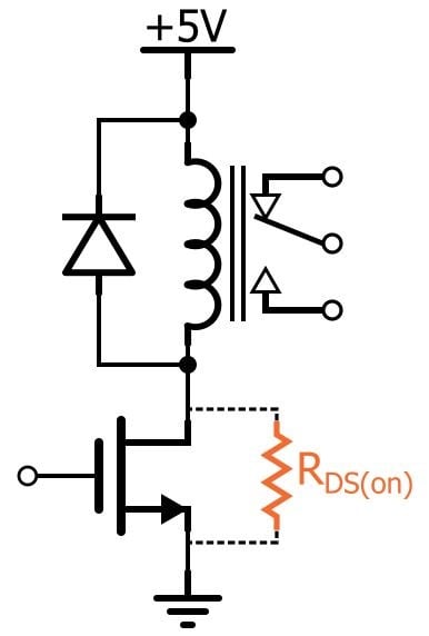
A third type of dV/dt failure is associated with the FET’s body diode. As you know, inductive loads need flyback diodes to provide a safe current path for inductive discharge. But it’s always nice to eliminate a component when possible and this makes us think about that diode so conveniently integrated into the FET. . . . I personally never rely on the body diode when it comes to flyback but, apparently, this is an acceptable design practice in some cases:

This diagram, taken from an ON Semi app note, depicts an arrangement in which FET body diodes are used as flyback diodes.
High dV/dt can cause “excessive diode recovery”, which refers to a rather complicated series of events that results in activation of the parasitic bipolar transistor mentioned above. I don’t know if this is always the case, but with the FCPF099N65S3, the maximum diode recovery dV/dt is lower than the maximum “MOSFET” (i.e., non-diode-recovery) dV/dt: the former is 20 V/ns and the latter is 100 V/ns. These are still extremely high dV/dt ratings, but it’s good to be aware that the device could be more sensitive to diode-recovery dV/dt than to typical static dV/dt.
I think that many of us have limited experience with truly high-power FET-based switching circuits. Various subtleties come into play—not just gate charge and dV/dt ratings but also temperature effects, such as temperature-related increases in on-state resistance or decreases in maximum drain current. If you have any helpful insights on this topic, feel free to share them in a comment.
Related Content