 Facebook
 Google
 GitHub
 Linkedin
Switching Losses: Effects on Semiconductors
We review switching losses involving diode recovery charge, transistor switching with clamped inductive load, device capacitance and leakage, package, and stray inductances, and the efficiency versus switching frequency curve.
We review switching losses involving diode recovery charge, transistor switching with clamped inductive load, device capacitance and leakage, package, and stray inductances, and the efficiency versus switching frequency curve.
Recommended Level
Beginner
Diode Recovery Charge
The switching characteristics of the diode during turn-off time is shown in Fig. 1.
.png)
Figure 1. Turn-Off Characteristics of Power Diode: a) Variation of the Current if ; b) Variation of the Voltage Drop vf ; c) Variation of the Power Loss
If we apply a reverse voltage across the diode, current through the diode comes to zero value, and the diode continues to conduct in the opposite direction because of the presence of stored charges in the depletion layer and the p or n layer. The diode current flows for a reverse recovery time trr. This is the time between when the instant forward diode current becomes zero and the instant reverse recovery current decays to 25 % of its reverse maximum value.
Time Ta: Charges stored in the depletion layer removed.
Time Tb: Charges from the semiconductor layer is removed.
Total recovery time:
$$T_{RR}=T_{a}+T_{b}$$
Peak reverse current:
$$I_{RM}=T_{a}\frac{di}{dt}$$ [Equation 1]
Reverse-recovery charge, QRRC, is the amount of charge that flow through the diode when diode changes its state from forward conduction mode to reverse blocking mode. This is given by the area enclosed below the x- axis by the path of current.
Thus,
$$Q_{RRC}≅\frac{1}{2}I_{RM}\,x\,T_{RR}$$
$$\Rightarrow I_{RM}=\frac{2Q_{RRC}}{T_{RR}}$$ [Equation 2]
From Equations 1 and 2, we get,
$$T_{RR}T_{a}=\frac{2Q_{RRC}}{\frac{di}{dt}}$$ [Equation 3]
Usually,
$$T_{b} << T_{a}.$$
Thus,
$$T_{RR}≈T_{a}$$ [Equation 4]
From Equations 3 and 4, we get,
$$T_{RR}≅\sqrt{(\frac{2Q_{RRC}}{\frac{di}{dt}})}$$ [Equation 5]
From Equations 5 and 2, we get,
$$I_{RM}=\sqrt{(2Q_{RRC}\frac{di}{dt})}$$ [Equation 6]
From a practical point of view, one is more concerned about the TRR and IRM which are clearly dependent on the stored charge QRRC and reverse applied $$\frac{di}{dt}$$ from Equations 5 and 6.
Transistor Switching having Clamped Inductive Load
Power BJT
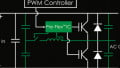
The delay in time during turn on or turn off is due to the time taken by the minority carrier to reach suitable density point. Its switching characteristics are specified in relation to external load circuit and the waveform for the base current. The clamped inductive switching circuit with flat base drive is shown in Fig.2.
.png)
Figure 2. Circuit for Switching Power BJT
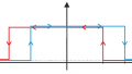
The key point for the power BJT is the storage time and switching losses. Switching losses occurs during turning on and turning off time and they dominate for the fast-switching operations. Waveforms showing change in the voltage and current during transition for resistive and inductive load is shown in Fig. 3.
.png)
Figure 3. Transition of the Voltage and Current during Turning-Off for (a) Inductive Load (b) Resistive Load
Complete inductive load switching characteristics for the power BJT is shown in Fig. 3
A base current should be high enough to ensure that the BJT turns quickly for the fast-switching operations. It should be maintained at a certain level after turning it on to keep it in the saturation state so as to minimize the conduction losses. As in case of power diode, reverse recovery time is dependent on the stored charge and the slope of the current.
Turn-on time for power BJT can be reduced by increasing the rate of the rise of the base current.
.png)
Figure 4. Power BJT Switching Characteristics for the Inductive Load
MOSFET
If the load current is constant over the switching interval of small duration and also due to inductive load; it can be considered as a constant-current source.
The switching circuit with the clamped inductive circuit in the case of the power MOSFET is shown in Fig. 5. The gate is driven by an ideal step-voltage source. Also, diode is taken to be ideal and thus not showing any reverse recovery characteristics.
.png)
Figure 5. Switching Circuit for MOSFET with Clamped Inductive Load
As the gate voltage is applied, it starts to rise towards VGG having time constant = RG (CGS + CGD)
.png)
Figure 6. Variation of CGS and VGD with VDS
The gate source capacitance of a MOSFET is the greatest among all the internal capacitances of MOSFET. The gate-to-drain transfer capacitance of a MOSFET has a large value in the ohmic region and then decreases to small value in the active region. The above graph clearly shows the variation of this capacitance with VDS. The switching characteristics for power MOSFET during turn-on and turn-off time are shown in Fig. 7 and Fig.8 respectively.
.png)
Figure 7. Turn-On Characteristics for Power MOSFET
.png)
Figure 8. Turn-Off Characteristics for Power MOSFET
IGBT
Switching circuit for IGBT with clamped inductive load is shown in Fig.9.
Turn-on and turn-off characteristics for the clamped inductive load is shown in Fig.10 and Fig.11. IGBT passes through active region during turning on and turning off time. Let the time constant of the inductive load i.e. $$T=\frac{L}{R}$$ be large enough such that load current is assumed constant during steady-state condition.
.png)
Figure 9. Switching Circuit for IGBT with Clamped Inductive Load
.png)
Figure 10. IGBT Switching Characteristics during Turn-On
During the turning on of an IGBT, the rate of fall of its voltage slows down toward the end since the output of p-n-p transistor follows its active region more slowly compared to the MOSFET.
.png)
Figure 11. IGBT Switching Characteristics during Turn-Off
During the turning off of the IGBT, a current tail may be created due to stored excess charges. When the IGBT is turned off, the gate-to-emitter voltage is kept at a negative value to avoid the latch up.
Device Capacitance: It is the internal capacitance that comes in parallel with the switch such as IGBT and MOSFET as shown in Fig. 5 and Fig. 9 when the switch comes in turning-on state. The energy stored is vanished during the turning on transition. Total energy stored in the capacitor is given by,
$$E_{c}=\sum_{i=0}^{n}\frac{1}{2}C_{i}{V_{i}}^{2}$$
Stray Inductances: These are inductances that appear effectively in series with switch when it starts to become open circuit. This stored energy is vanished during the turn-off transition.
$$E_{L}=\sum_{i=0}^{n}\frac{1}{2}L_{i}{I_{i}}^{2}$$
Besides this losses during the turn-on and turn-off transitions, there may be switching losses due to diode stored charge, parasitic capacitances, parasitic inductances and ringing.
Efficiency vs. Switching Frequency
Power is proportional to the energy stored multiplied by the frequency. Efficiency of a converter decreases with the increase of the switching frequency. But, there exist a certain critical value of a frequency which the efficiency decreases drastically.
.png)
Figure 12. Efficiency vs Switching Frequency Curve


“reverse voltage across the diode, current through the diode comes to zero value, and the diode continues to conduct in the opposite direction”
Does “opposite direction” here mean “forward voltage”? “reverse voltage”? Something else?
thx
Confused by Figure 1, cuz it looks like current changes before voltage. i thought voltage changes first?