Facebook
 Google
 GitHub
 Linkedin
Trim Out ADC Offset and Gain Error Using Two Point Calibration
Learn about the two-point calibration method and the fixed-point implementation to compensate for analog-to-digital converter (ADC) offset and gain errors through an example.
In a previous article, we discussed that a single-point calibration could be used to trim out the ADC offset error. To compensate for both the offset and gain errors, we need a two-point calibration. In this article, we’ll explore the two-point calibration method and learn about the fixed-point implementation of this technique through an example.
Two-point Calibration Testing to Determine Actual ADC Offset and Gain Error
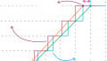
Figure 1 shows the characteristic curve of a unipolar 12-bit ADC that is affected by offset and gain errors.
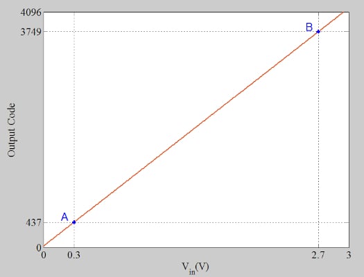
Figure 1. A characteristic curve of a unipolar 12-bit ADC affected by offset and gain errors.
The full-scale value of the ADC is 3 V. Two test inputs at 10% and 90% of the full-scale range of the ADC, points A and B, are chosen to determine the ADC offset and gain errors. At 0.3 V and 2.7 V, the measured output codes are 437 and 3749, respectively. The slope of the measured transfer function can be calculated as:
\[Slope_{m}=\frac{Code_{B}-Code_{A}}{V_{in,B}-V_{in,A}}=\frac{3749-437}{2.7-0.3}=1380\frac{Count}{V}\]
Using the x and y values of point A, we obtain the following line equation:
\[y_{m}=1380(V_{in}-0.3)+437\]
By substituting Vin = 0, the offset error is found to be +23 LSB. The equation below describes the linear model of an ideal 12-bit ADC:
\[y_{_{ideal}}\frac{V_{in}}{FS}\times2^{N}\]
Therefore, the ideal code values at 0.3 V and 2.7 V are 409 and 3686, respectively. Using these values, the slope of the ideal response is obtained as:
\[Slope_{i}=\frac{Code_{B,i}-Code_{A,i}}{V_{in,B}-V_{in,A}}=\frac{3686-409}{2.7-0.3}=1365.42\frac{Count}{V}\]
Now we can calculate the gain error of the ADC as follows:
\[Gain\,Error=\frac{Slope_{m}-Slope_{i}}{Slope_{i}}=\frac{1380-1365.42}{1365.42}=0.011=1.1\%\]
Two-point Calibration—Trimming Out ADC Offset Error and Gain Error
Knowing the actual response, we can now easily trim out the offset and gain errors in the digital domain. First, we can subtract the offset from every output code to arrive at a response that goes through the origin and has a slope of Slopem. Next, multiplying the result by \(\frac{Slope_{i}}{Slope_{m}}\) rotates the obtained line about the origin and produces a straight line with a slope of Slopei.
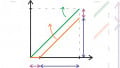
These mathematical operations map the straight line of the actual response to that of the ideal ADC. Figure 2 uses an exaggerated example to illustrate the calibration concept.
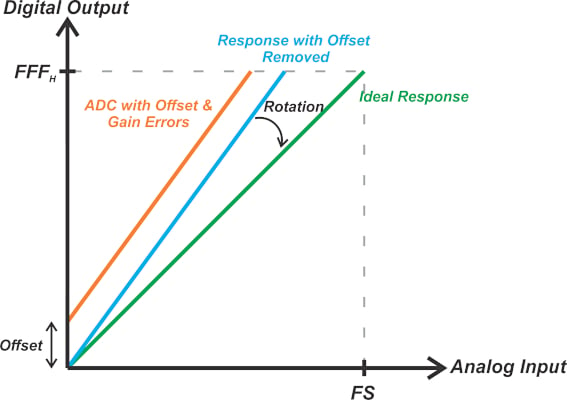
Figure 2. An example response to show the ADC calibration.
Therefore, the calibrated output code, CodeCal, can be calculated from the actual code, Codea, by applying Equation 1:
\[Code_{Cal}=(Code_{a}-offset)\times\frac{Slope_{i}}{Slope_{m}}\]
Equation 1.
Fixed-point Calibration Implementation
On the other hand, if we are trying to compensate for a fixed value of offset and gain error, we can simplify Equation 1 and achieve a more computationally-efficient system. Continuing with our example, we can substitute offset = 23, Slopei = 1365.42, and Slopem = 1380 into Equation 1 to obtain the following relationship:
\[Code_{Cal}=(Code_{a}-23)\times\frac{1365.42}{1380}\]
To save some CPU (central processing unit) cycles from the system processor, we can simplify the above equation as Equation 2:
\[Code_{Cal}=c_{1}\times Code_{a}+c_{2}\]
Equation 2.
Where:
- c1 = 0.989434782
- c2 = -22.757
Though we can use floating-point arithmetic to implement the above equation, a fixed-point implementation can be more efficient and cost-effective. We have two fractional numbers, c1 and c2. To represent fractional numbers in a fixed-point format, we'll use an implied binary point. This means that we'll assume that a certain number of bits of the register represent the integer part, whereas the remaining bits represent the fractional part of the number.
The Q format notation is then used to specify the number of bits of the integer and fractional parts. For example, 101.0011 can be a number in Q3.4 format as it uses three bits for the integer and four for the fractional part.
Note that the binary point is not actually implemented in hardware; it’s only a concept that allows us to represent fractional numbers in a fixed-point processor. Additionally, a number in a given Q format might represent either a positive or negative value.
Returning to our ADC calibration example, we have two fractional numbers, c1 and c2, that should be represented in an appropriate fixed-point format. Let's assume that signed 16-bit registers in two’s complement format are used to store these constants. Since c1 is less than 1, the integer part needs only one bit for the sign. The remaining bits can represent the fractional part, leading to the Q1.15 format.
To find the fixed-point representation of c1, we multiply it by 215, round it to the nearest integer, and convert the rounded result into the binary form.
\[c_{1,new}=c_{1}\times2^{15}=32421.8\simeq32422=0111\,\,1110\,\,1010\,\,0110_{2}\]
Since c2 is between 16 and 32, we need 5 bits for the integer part and one for the sign. This leaves us with 10 bits for the fractional part. Therefore, the appropriate representation for c2 is the Q6.10 format. To represent in this format, we multiply c2 by 210, round it to the nearest integer, and convert the rounded result into the binary form.
\[c_{2,new}=c_{2}\times10^{10}=-23303.2\simeq-23303=1010\,\,0100\,\,1111\,\,1001_{2}\]
Note that c2 is a negative number in two’s complement format. Since the new coefficients use different scaling factors, we need to carefully keep track of the effect of the scaling factors on our calculations. Let’s define a new temporary variable, Var1, to store the product of c1, new and the uncalibrated ADC reading as Equation 3:
\[Var_{1}=c_{1,new}\times Code_{a}\]
Equation 3.
This produces the first term on the right side of Equation 2. Assume that the 12-bit output of the ADC is stored in a signed 16-bit register in our C program. Therefore, Codea can be considered a Q16.0 number. This means that implementing Equation 3 requires multiplying a Q1.15 value by a Q16.0 one. The variable Var1 should be a 32-bit register to store the result of this multiplication. Besides, since a Q16.0 number is multiplied by a Q1.15 value, Var1 is in Q17.15 format. If you need to brush up on multiplication using fixed-point representation, please refer to this article.
As you can see, the multiplication operation increases the data word length. When implementing DSP (digital signal processor) algorithms, we commonly truncate or round the multiplication output to prevent the word length from growing without limit. However, before truncating or rounding the multiplication output, we should consider the next operation on the data.
In this example (Equation 2), the multiplication result will be added to c2, new, which is in Q6.10 format. Considering the fractional part of c2, new, we can discard the five least significant bits of Var1 and store the truncated result in a new variable Var2. The right-shift operator in C programming can be used to perform this:
\[Var2=Var1>>5;\]
Equation 4.
If we had arbitrary register lengths in our system (for example, as we have in FPGAs), we could store Var2 using a 27-bit register in the Q17.10 format. However, in C programming, Var2 still has to be stored in a 32-bit register. If we truncate the five least significant bits of a Q17.15 number and store the result in a 32-bit register, we’ll obtain a Q22.10 number. Finally, we can add c2, new to Var2, and discard the 10 least significant bits to arrive at the calibrated ADC value, getting Equation 5:
\[CodeCal=(Var2+c2new)>>10;\]
Equation 5.
As a side note, to avoid any confusion, I’d like to mention that the variables in Equations 4 and 5 do not use subscripts, as these two lines are assumed to be pseudocodes. For example, Var2 in the text is written as Var2 in Equations 4 and 5.
ADC Fixed-point Calibration Verification
Let’s see if the above fixed-point coefficients (c1, new = 32422 and c2, new = 23303) can map the measured ADC response to the ideal straight-line model. At point A in Figure 1, the ADC output is 437. Applying Equation 3, Var1 is found as:
\[Var_{1}=32422\times437=14168414\]
Converting this to the binary format, right-shifting by 5 bits, and then finding the decimal equivalent, we obtain:
\[Var_{2}=442762\]
Now, we add c2, new, and right-shift the binary equivalent of the result by 10 bits, which yields:
\[Code_{Cal}=409\]
You can similarly verify that point B is also mapped to the ideal code 3686. Note that the computer program uses the binary equivalent of the coefficients, I just used the decimal values to clarify the calculations. We can similarly check other points from the measured ADC response to ensure that the fixed-point implementation produces the desired values. If this is not satisfied, we’ll have to use larger registers for storing the calibration coefficients.
ADC Unused Output Code and Input Range
Previously, we discussed that offset and gain errors can lead to unused output codes. The calibration technique discussed above is performed after the A/D conversion. As a result, it cannot solve the unused code problem. To clarify this, consider the example shown in Figure 3.
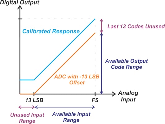
Figure 3. Example showing the unused and available input ranges and output code ranges.
In this example, a unipolar ADC with an offset of -13 LSB is shown. The offset error can be calibrated out by adding 13 to the ADC readings. However, notice that the ADC outputs the all-zeros code for input values less than 13 LSB. This input range will still be unavailable in the calibrated response because calibration is performed after the A/D conversion. The calibration only adds a constant offset to the actual ADC response, producing code 13 for all values below 13 LSB in the above example. It should be noted that some ADCs have built-in calibration functions that are different from the post-conversion method discussed in this article. These built-in calibration techniques might be able to retain the native range of the ADC. Such a built-in calibration technique is used in the 12-bit ADC found on the TMS320280x and TMS3202801x devices from TI.
Featured image used courtesy of Pixabay
To see a complete list of my articles, please visit this page.