Facebook
 Google
 GitHub
 Linkedin
System Calibration and Background Calibration in Precision ADCs
Learn about two calibration functions in precision ADCs: system calibration and background calibration modes.
In a previous article, we looked at the self-calibration functions that are supported by some precision analog-to-digital converters (ADCs). We also discussed that, in addition to the internal errors of the ADC, the external circuitry can also produce significant offset and gain errors in our measurements.
This article examines two other calibration functions that are implemented in some precision ADCs, namely system calibration and background calibration modes.
Remove Offset and Gain Errors Via System Calibration
While self-calibration compensates for the ADC internal errors, system calibration functions attempt to remove the offset and gain errors of the whole system. The self-calibration functions internally provide the required voltages at the ADC inputs, whereas system calibration requires the user to externally apply the appropriate inputs to the ADC. In addition, system calibration can include system offset and gain calibration functionalities.
As previously discussed, many ADCs use a variant of the following calibration scheme where the value of the offset calibration register (OFC) is first subtracted from the output of the A/D conversion process, and then, the result is multiplied by the gain calibration value (FSC register), as shown below in Figure 1.
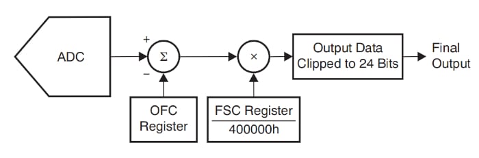
Figure 1. Example block diagram showing an ADC, OFC register, and FSC register. Image used courtesy of TI
System Offset Calibration
As for system offset calibration, the user externally applies zero volts to the ADC inputs and runs the system offset calibration routine. The calibration function attempts to compensate for any offset produced by the board and the ADC internal circuitry. Figure 2 illustrates system offset calibration for the EVAL-AD7124-4SDZ evaluation board.
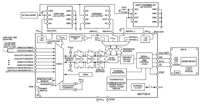
Figure 2. Offset calibration for EVAL-AD7124-4SDZ. Image used courtesy of Analog Devices
Note that the ADC inputs AIN0 and AIN2 are shorted externally. While the AD7124-4 has a typical uncalibrated offset of ±15 μV, the above system exhibits 24 μV offset without calibration. After performing system offset calibration, the analog equivalent of the ADC output code for zeroed input is about 120 nV, which is in the order of the ADC noise.
System Offset Error Sources
You might ask: what effect makes the above simple system have an offset of 24 μV while the ADC offset is only ±15 µV? However, since the ADI document doesn’t elaborate on this, it seems to that the source of this additional offset can be the board parasitic thermocouples.
A thermocouple is created when two dissimilar metals are joined at a junction. This inevitably happens in normal circuit wiring (e.g. at the junction between tin-lead solder and a copper PCB trace), which thus creates a parasitic thermocouple with a Seebeck coefficient of 3 to 4 μV/°C. Parasitic thermocouples also exist at the junction of the copper PCB traces and the Kovar pins of the ICs. These junctions exhibit a Seebeck coefficient of about 35 μV/°C.
As you can see, a small temperature gradient across the board can create a thermocouple voltage that is comparable with the uncalibrated offset of a precision ADC. Therefore, signal paths for the two analog inputs should be kept identical and close to each other. With matched input lines, the thermocouple effect should ideally lead to a common-mode voltage at the ADC input, which will be attenuated by the common mode rejection ratio (CMRR) of the ADC.
While identical signal paths can minimize the thermocouple effect, they cannot totally eliminate it, as a temperature gradient might exist across the board. However, if this temperature gradient is constant, a system calibration can eliminate the remaining offset error. In addition to the parasitic thermocouples, amplifiers and filters in the signal path can contribute to the system offset error.
As an example, consider the circuit diagram below in Figure 3.
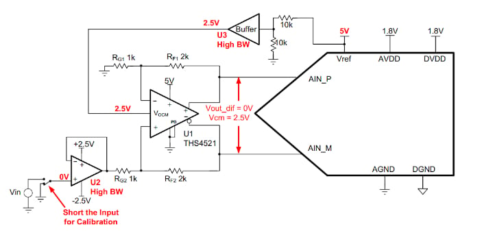
Figure 3. Example circuit diagram showing the input for calibration. Image used courtesy of TI
Again, for offset calibration, the input is disconnected from the signal source and shorted to ground through the switch. In this example, the offset from the amplifiers U1 and U2 and the ADC offset contribute to the overall system offset. These offset terms, as well as the thermocouple effects, can be calibrated out using system offset calibration. If the offset temperature drift associated with the front-end signal conditioning circuitry limits the performance, we’ll need to repeat the system calibration whenever the operating temperature changes significantly.
System Gain Calibration
System gain calibration corrects for gain error in the signal path. In a system gain calibration, the inputs are externally connected to an appropriate positive full scale, depending on the PGA gain and the reference voltage. For example, consider system gain calibration for the EVAL-AD7124-4SDZ evaluation board (Figure 4).
Figure 4. Block diagram showing the system gain calibration for EVAL-AD7124-4SDZ. Image used courtesy of Analog Devices
In this example, the reference voltage is 2.5 V. If the PGA gain is 2 and the AD7124-4 is configured for bipolar mode, a full-scale voltage of 1.25 V should be applied to the module inputs. Due to different gain error contributors, the 1.25 V input might not produce the full-scale output code without calibration. During system gain calibration, the ADC assumes that the full-scale voltage is applied to the inputs. Thus, the calibration function maps the code produced by the A/D conversion process to the ideal full-scale code at the ADC output. As another example, consider the 3-wire, ratiometric RTD measurement system below in Figure 5.
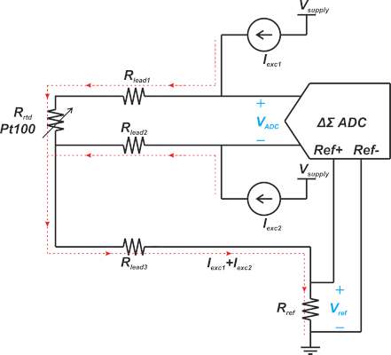
Figure 5. Three-wire ratiometric RTD measurement system diagram.
Assume that the maximum temperature that the RTD will measure is 814 °C. To produce the full-scale signal for the ADC, we can replace the RTD with a 0.01%, 380Ω resistor as this resistance corresponds to approximately 814 °C with a PT100 RTD. With the calibration resistor in place, we can use the ADC system calibration function to trim out the gain error. For higher accuracy, however, we might decide to manually determine the value of the gain calibration register rather than relying on the ADC system calibration function. Manual gain calibration allows us to take into account factors such as the tolerance of the calibration resistor and the fact that 814 °C actually corresponds to 379.871 Ω rather than 380 Ω. With manual gain calibration, we can measure the actual value of the calibration resistor using an 8.5-digit multimeter and calculate the gain calibration coefficient that maps the output code to the ideal full-scale code.
System Gain Error Sources
In addition, to gain error from the ADC itself, there can be several other gain error contributors depending on the application. In the example illustrated in Figure 4, the initial accuracy of the voltage reference leads to a gain error in the ADC transfer function. You can verify that if the reference voltage tolerance specified as a percentage is x, the gain error from the voltage reference tolerance is also about x percent. For example, a reference voltage with an initial accuracy of 0.05% leads to about 0.05% gain error in the ADC transfer function.
With a more complicated signal chain such as the one in Figure 3, the gain error of the amplifiers and filters will also contribute to the system gain error. As another example, consider the RTD application in Figure 5. In this case, the tolerance of Rref, the mismatch between the current sources, and the ADC gain error are the three main contributors to the system gain error.
Final Thoughts on System Calibration
As discussed above, appropriate input voltages should be externally applied to the ADC for system calibration. It should be noted that these inputs should be applied before the system calibration step is initiated and must remain stable until the step is complete. Without stable inputs, the ADC cannot accurately determine the calibration coefficients.
Considering the drift performance of the signal chain components and the temperature range over which the system operates, you might need to increase the frequency of calibrations depending on the application’s accuracy requirement.
Background Calibration
This is another type of self-calibration which is found in some ADCs, such as the AD7714 from Analog Devices. With background calibration, the calibration procedure is interleaved with the normal conversion sequence. After every output update, the AD7714 performs a zero-scale self-calibration. This reduces the output data rate of the ADC by a factor of 6; however, it enables the device to continually remove the effects of temperature drift, supply sensitivity, and aging on the zero-scale error.
The LMP90100 from TI is also a good example of a device that includes background calibration. With conventional background calibration methods, the ADC input has to be interrupted while the ADC is calculating the offset or gain coefficients. However, the LMP90100 uses a different calibration technique (with some assumptions about the input signal) that leads to minimal impact on the output data rate of the ADC. For more information about this device, please refer to this application report.
Featured image used courtesy of Wikipedia
To see a complete list of my articles, please visit this page.
Related Content