Facebook
 Google
 GitHub
 Linkedin
Understanding CMRR and its Relationship With ADC Offset Error
Learn how variations of the common mode rejection ratio (CMRR) can affect an analog-to-digital converter's (ADC) performance.
In different applications, such as sensor measurement systems and communication systems, we observe that the common mode signal at the ADC input is not constant. Variations in the common mode voltage can be due to a noise component that equally couples to both inputs of the ADC or stem from the normal circuit operation.
In this article, we’ll see how variations of the common mode level can affect the ADC's performance.
Why is the ADC Common Mode Rejection Important?
Figure 1 shows a simplified diagram for RTD measurement.
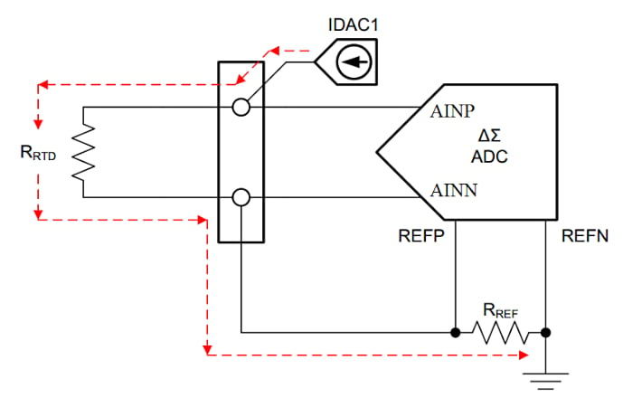
Figure 1. Example diagram of an RTD measurement. Image used courtesy of TI
In the above example, the excitation current source forces a fixed current to flow through the RTD and the reference resistor RREF. The voltage across the RTD is directly measured by the ΔΣ (delta-sigma) ADC. The voltage across RREF is also used to provide the reference voltage of the ADC, leading to a ratiometric measurement.
In addition to providing the reference voltage, RREF level shifts the RTD voltage to be within the specified input common mode range of the ADC. Let’s consider some typical values for a 100 Ω platinum RTD system. Assume that the ADC is operated with a single 3.3V supply and the excitation current is 1 mA. Normally, the mid-supply is within the common mode range of the ADC. Based on this assumption, we can use RREF = 1.6 kΩ to level shift the RTD signal to 1.6 V, which is close to the midpoint of the supply voltage.
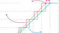
Next, let's assume that the RTD temperature changes from -100 °C to 400 °C, changing the RTD resistance from 60.256 Ω to 247.092 Ω. In this example, the AINN input remains at 1.6 V, whereas the AINP input changes from about 1.66 V to 1.847 V over the specified temperature range. If we assume that temperature variations follow a sinusoidal waveform in our hypothetical application, the voltages of AINN and AINP resemble the waveforms shown in Figure 2.
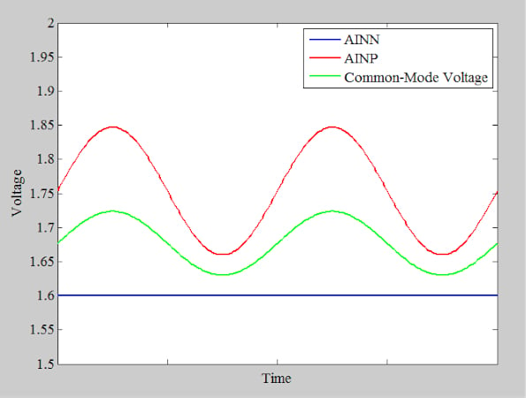
Figure 2. Example application graph showing voltage vs. time for AINN, AINP, and common mode voltage.
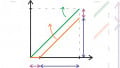
The green curve in the above figure shows the average value of AINN and AINP, which is the common mode voltage experienced by the inputs. In this example, the common mode voltage is not constant and changes by about 100 mVp-p. In an ideal world, this should not be an issue. An ideal differential ADC measures the voltage difference between its two inputs and completely eliminates any common-mode signal, as illustrated in Figure 3.
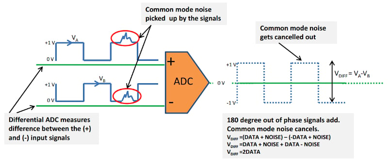
Figure 3. An example ADC measuring the voltage difference between its two inputs, eliminating common mode signals. Image used courtesy of Microchip
With a real-world ADC, however, the common mode signal is only attenuated rather than completely rejected. The common mode rejection ratio (CMRR) is an important specification that characterizes the ADC's ability to prevent a common mode signal from appearing at the ADC output.
ADC Common Mode Rejection Ratio Equations
The conventional textbook definition of CMRR is the ratio of the differential-mode gain (Adiff) to the common mode gain (Acm) of the circuit. Mathematically, we get Equation 1:
\[CMRR=\frac{A_{diff}}{A_{cm}}\]
Equation 1.
In the context of ADCs, the differential-mode gain is the slope of the linear model of the ADC and is defined as the ratio of the change in the output code to the change in the differential input. Similarly, Acm is found by dividing the change in the output code by the change in the input common mode signal. Rather than the change in the output code, we can also use the analog equivalent of the change in the output code to find Acm, Adiff, and CMRR. The CMRR is usually expressed in dB using Equation 2:
\[CMRR(dB)\,=\,20log\Big(\frac{A_{diff}}{A_{cm}}\Big)\]
Equation 2.
As an example, the CMRR specification of the AD4030-24 is provided in the following table.
Table 1. Data used courtesy of Analog Devices
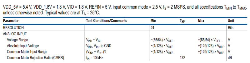
The device exhibits a CMRR of 132 dB for a common mode signal at 10 kHz. We’ll discuss shortly that an important test condition for the CMRR specification is the input common mode, at which the CMRR is measured. As you can see, the input common mode is 2.5 V for the AD4030-24 CMRR testing.
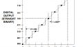
So, what does it mean that the AD4030-24 has a CMRR of 132 dB? This means that, by assuming Adiff = 1, the AD4030-24 attenuates the input common mode signal by 132 dB at the output. Note that the CMRR specification is frequency-dependent. Datasheets usually provide the plot of the device CMRR versus frequency. Figure 4 shows how the CMRR of the AD4030-24 changes with frequency.
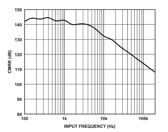
Figure 4. Change of frequency in the CMRR of the AD4020-24. Image used courtesy of Analog Devices
Below 10 kHz, the device can provide even greater than 132 dB of CMRR. If you’re considering the performance at a specific frequency, you should consider the CMRR at that frequency.
Input Error From Common Mode Variations
In addition to the equations discussed above, we can derive another useful equation by referring to the error produced by the common mode variations to the ADC input. Let's assume that the input common mode voltage changes by ΔVcm, which causes the output code to change by a certain value. If the analog equivalent of the change in the output code is ΔVout, we get:
\[A_{cm}=\frac{\Delta V_{out}}{\Delta V_{cm}}\]
We can say that changing the input common mode by ΔVcm produces an unwanted error of ΔVout at the ADC output. To refer this error to the input, we can divide it by the ADC differential-mode gain, which yields:
\[Input\,Referred\,Error=\frac{|\Delta V_{out}|}{A_{diff}}=\frac{A_{cm} |\Delta V_{cm}|}{A_{diff}}\]
By substituting Equation 1 into the above equation, we obtain Equation 3:
\[Input\,Referred\,Error=\frac{|\Delta V_{cm}|}{CMRR}\]
Equation 3.
This means that the effect of changing the common mode voltage by ΔVcm can be modeled by an error term equal to \(\frac{|\Delta V_{cm}|}{CMRR}\) at the ADC input.
Note that we used the CMRR definition provided by Equation 1 to derive the above equation. If the CMRR is given in dB, we should first use Equation 2 to find the equivalent CMRR value in V/V and then apply Equation 3.
Let’s look at an example.
Common Mode ADC Measurement Example:
Assume that different DC specifications of an ADC, including the CMRR parameter, are measured at a common mode input of 2.5 V. The minimum CMRR of the ADC is 100 dB for low-frequency common mode signals. In our application, the following signals are applied to the ADC differential inputs:
\[V_{AINN}=3.5-0.1sin(2\pi t)\]
\[V_{AINP}=3.5+0.1sin(2\pi t)\]
As you can see, the ADC is used at a common mode level different from the test condition specified in the datasheet. How is this going to affect the performance?
In this example, the common mode input is 3.5 V rather than the 2.5 V used in the datasheet measurements. Changing the common mode input by \(|\Delta V_{cm}|=1\) produces an input-referred error term that can be found as follows (Equation 3):
\[Input\,Referred\,Error=\frac{|\Delta V_{cm}|}{CMRR}=\frac{1}{10^{(\frac{100}{20})}}=10\mu V\]
Note that a CMRR of 100 dB yields \(\frac{A_{diff}}{A_{cm}}=10^{5}\frac{V}{V}\), which is used in the above equation.
This example shows that changing the input common mode voltage by a fixed value leads to a constant input-referred error. In other words, we can model a constant change in the common-mode value by a change in the ADC offset error. In the above example, if the datasheet offset error (specified at input common mode voltage of 2.5 V) is ±30 µV, now we expect it to increase to ±40 µV.
A constant offset error can be easily calibrated out at the ADC output. However, a varying common mode voltage leads to a varying error at the ADC input. Common mode variations can be caused by a common mode noise, such as the 50/60 Hz noise from powerlines, or they can simply stem from the normal operation of our system, as in the case of the RTD measurement system discussed at the beginning of the article.
A Word About an ADC Input Common Mode Range
Different ADCs are designed to support different input common mode ranges. The input common-mode range of many fully-differential successive approximation register (SAR) ADCs is limited to a small range around VREF/2. A typical range is (VREF/2) ±100 mV. In these cases, we need to keep the output common mode of the preceding stage within the common-mode range of the ADC. Figure 5 shows how a fully-differential amplifier (FDA) that features an output common mode pin (Vocm) can be used to fix the common mode level of the FDA output at VREF/2.
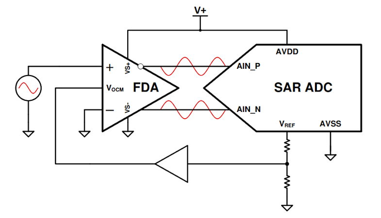
Figure 5. Diagram showing a fully-differential amplifier with an output common mode pin used to fix the common mode level. Image used courtesy of TI
There are also SAR ADCs with a wide input common mode range. An example (Figure 6) of this type is the LTC2311-16 from Analog Devices.
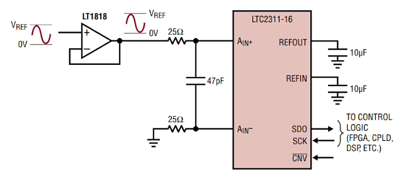
Figure 6. Block diagram for the LTC2311-16. Image used courtesy of Analog Devices
The wide input common mode range of this device allows different input configurations, such as the pseudo-differential unipolar configuration shown below. Note that the input common mode changes from 0 to VREF/2 in this example.
On the other hand, most ΔΣ ADCs are designed to provide a relatively larger input common mode range than that of SAR ADCs. Since many ΔΣ ADCs have built-in programmable gain amplifiers (PGAs), it should be noted that the common mode range of the ADC can be smaller if we configure the PGA to operate at a higher gain.
ADC Power Supply Rejection Ratio (PSRR)
The power supply rejection ratio (PSRR) is the ability of the ADC to reject power supply variations. Similar to the CMRR effect, the effect of finite PSRR can be modeled as an error source at the ADC input. In this case, the input-referred error is given by:
\[Input\,Referred\,Error=\frac{|\Delta V_{ps}|}{PSRR}\]
Where \(|\Delta V_{ps}|\) denotes the variation in the supply voltage.
To see an example of calculating the PSRR error, please refer to this TI presentation.
To see a complete list of my articles, please visit this page.