 Facebook
 Google
 GitHub
 Linkedin
CCD Image Sensor Types: Full-Frame, Interline-Transfer, and Frame-Transfer CCDs
This article explains the characteristics, advantages, and disadvantages of three CCD (charge-coupled device) architectures.
In the previous article, we looked at the general structure of CCDs at the semiconductor level. The two most fundamental elements of any CCD image sensor are the photoactive area (such as a pinned photodiode) and the charge-transferring structures (i.e., horizontal and vertical shift registers). But these elements can be organized and implemented in different ways, and consequently “CCD” is a general image-sensor category that consists of several subcategories.
In this article, we’ll examine the full-frame (FF), frame-transfer (FT), and interline-transfer (IT) CCD architectures.
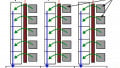
Full-Frame CCDs
I find it somehow counterintuitive that a semiconductor region could function as both a photoactive element and a charge-transfer device, but that’s exactly what happens in FF CCDs. During integration, the pixel location accumulates electric charge in response to incident photons. After integration, the charge packets are moved vertically through the pixel locations toward the horizontal shift register.
As we know from the previous article, we obtain CCD pixel data by applying carefully timed clock signals that sequentially create potential wells and potential barriers in the charge-transferring structure of the device. In a full-frame CCD, we need to be able to apply these control voltages to regions that also function as photodetectors. Thus, gate electrodes are made from transparent polysilicon.
Full-frame CCDs are (relatively) straightforward and (relatively) easy to fabricate, and they allow the entire CCD surface to be light sensitive. This maximizes the number of pixels that can be included in a given area of silicon, and it also maximizes the portion of each pixel that is actually capable of converting photons into electrons.
However, a major limitation is the need for a mechanical shutter (or a synchronized, short-duration light source called a strobe). The photoactive areas of the CCD don’t stop being photoactive simply because you have decided that it’s time to perform readout. Without a mechanical shutter that blocks incoming light after the exposure period is complete, the charge packets generated during (intentional) integration would be corrupted by light that arrives during readout.

This is the basic architecture of a full-frame CCD.
Frame-Transfer CCDs
In general, we prefer to control exposure electronically. A shutter (like any other rapidly moving, high-precision mechanical device) makes the design more complex, the end product more expensive, and the overall system more subject to failure. The additional energy required to actuate a physical object is also undesirable in battery-powered applications.
An FT CCD allows us to maintain some of the benefits of the FF CCD while (almost) eliminating the need for a shutter. This is accomplished by dividing an FF CCD into two equally sized sections. One of these sections is the normal light-sensitive imaging array, and the other is a storage array that is shielded from incident light.
After integration, charge packets for all of the pixels are rapidly transferred to the storage array, and then readout occurs in the storage array. While the storage locations are being read out, the active pixels can be accumulating charge for the next image, and this allows frame-transfer CCDs to achieve higher frame rates than full-frame CCDs.
I say that the FT architecture almost eliminates the shutter because shutterless designs are subject to a problem called vertical smear. The transfer of charge packets from active pixels to storage locations occurs quickly, but not instantaneously, and consequently image information can be altered by light that reaches the sensor during the vertical transfer period.
Major disadvantages of the FT architecture are higher cost and increased area relative to image quality, since you’re basically taking an FF sensor and then reducing the number of pixels by a factor of two.

The frame-transfer CCD adds a storage array to the full-frame architecture.
Interline-Transfer CCDs
The last major architectural improvement that we need is some method of transferring integrated charge to a storage area so rapidly that smear is reduced to negligible levels. The interline-transfer CCD accomplishes this by providing a network of storage (and transfer) regions that are adjacent to each photoactive location. When exposure is completed, every charge packet in the sensor is simultaneously transferred into non-light-sensitive vertical shift registers.
Thus, IT CCDs enable electronic shuttering with minimal smear, and like FT CCDs, they can integrate during readout, thereby maintaining the higher frame-rate capability. However, some smear can occur if light-generated charge from the photoactive columns leaks into an adjacent vertical shift register during readout. If the application doesn’t require high frame rates, this problem can be eliminated by delaying integration until readout is complete.
Interline CCDs don’t require the large storage section used in frame-transfer CCDs, but they introduce a new disadvantage: the sensor becomes a less efficient means of converting photons to electrons, because each pixel location now consists of a photodiode and a portion of a vertical shift register. In other words, part of the pixel is not sensitive to light, and therefore less electric charge is generated relative to the amount of light falling on the pixel area. This loss of sensitivity is greatly mitigated by fabricating the sensor with the addition of tiny lenses that concentrate incident light onto the photoactive region of each pixel, but these “microlenses” come with their own set of difficulties.

In the interline-transfer architecture, the storage (and vertical transfer) area is located between photoactive columns.
Conclusion
I hope that this article helps you to understand the trade-offs involved in the design of a CCD image sensor. Full-frame CCDs might seem like the most “primitive” type, but I believe that they are still preferred in systems that don’t need high frame rates and that can tolerate the use of a strobe or mechanical shutter. Frame-transfer CCDs and interline-transfer CCDs are more versatile and offer crucial advantages in certain applications.


Can the interline transfer area be implemented below the active photo area? More of an “under-line” structure, fabricated on a layer below the photolayer?
Has anyone made a CCD that can sample the pixels continuously in time? Where every pixel has a unique time that it is collecting information?
I do not want whole frames or whole rows all collecting data at limited number of times, but every pixel each with its own time slot. I want to maximize data for time of flight calculations. A 1920x1080x30 fps device only collects 1080x30 rows per second. But the same device, if it could process pixels sequentially or randomly, could produce a time stamped stream of 1920x1080x30 pixel values per second. The difference is 299792458/1920*1080*30 = 4.819 meter radial resolution, rather than 299792458/1080*30 = 9.253 km resolution.
Any suggestions? Or do I have to wait for the CMOS articles? Surely someone must have made a sequential pixel reading chip??
Thank you for these articles. I look forward to more and longer ones.