 Facebook
 Google
 GitHub
 Linkedin
Understanding the Structure and Functionality of CCDs
This article will help you to understand what CCD sensors are and how they allow us to convert an optical scene into a digital image.
One of the first major projects that I worked on as a fledgling EE was a custom-designed digital camera built around an intimidating CCD sensor from Kodak. I wrote the firmware and handled all the readout control, and a senior engineer designed the hardware. We were pretty much a two-man team.
Initially, I had zero expertise in the low-level details of electronic imaging systems, but my supervisors opted for the sink-or-swim approach, and it paid off. The camera worked, and by the end of that project, I probably knew more about CCD timing than anyone else in the building.
What Is a CCD?
“CCD” stands for “charge-coupled device.” A CCD is an integrated semiconductor system that converts photons into electrons and then moves these light-generated packets of electric charge from their original location to the sensor’s output pin.
If you think that “charge-coupled device” is a strange name for an image sensor, you’re right. This term refers merely to a system of moving electric charge, so in this context, what we really mean when we say “CCD” is something like “charged-coupled light-sensitive device.”
Researchers initially studied CCDs as a new way of storing information in computer systems, and later they recognized that the technology could be useful in light-detecting applications. This probably explains why the term “CCD” denotes an imaging device yet doesn’t include any explicit reference to imaging.
CCD Structure
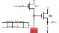
The following diagram gives you a general idea of how CCDs are constructed and what happens at the semiconductor level.

- A pixel’s photodiode produces electrical potential in response to incident light. The relationship between light intensity over time and accumulated charge is initially linear but becomes nonlinear as the pixel approaches saturation. Modern CCDs use pinned photodiodes, which include a thin p+ layer that is not shown in this diagram.
- Electrons accumulate in a “potential well” within the p-type silicon underneath the diode.
- A potential well is a physical area created by applying a positive voltage. The term “well” is used because this positive voltage attracts electrons and repels holes, thereby creating a region into which the light-generated electrons will flow.
- We create a potential barrier by applying 0 V or a negative voltage. A barrier blocks the movement of electrons.
- Clock signals applied to transfer gates lead to the sequential generation of wells and barriers, and this is the fundamental mechanism by which a CCD directs discrete packets of light-generated charge from individual pixels to the sensor’s output terminal.
- The reset gate is a means of clearing the accumulated charge in a pixel. We’ll return to the reset and drain later in the article.
CCD Operation
The image-capture process begins in the photoactive region of each pixel. Following the period known as exposure (in reference to film that is exposed to light only when the camera’s mechanical shutter is open) or as integration (because the photodiodes are accumulating charge), each pixel has a quantity of electric charge corresponding to the light intensity at that particular pixel location.
We now have an electrical representation of the optical scene, but we have no direct access to these discrete packets of charge. We need to transfer them off the device so that they can be amplified, digitized, processed, and displayed as a two-dimensional image. This is where the charge-coupling activity comes in. By applying carefully timed control voltages to the sensor, we can move these charge packets—one by one, step by step—toward the output pin. This is called readout.
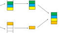
A CCD operates as a network of analog shift registers. A horizontal (aka serial) shift register moves charge packets from one line of the sensor to the output. When that line is complete, vertical (aka parallel) shift registers move charge packets for the next line into the horizontal shift register, which then performs readout. This process continues, with thousands or millions of little charge packets marching around the sensor until every last one has been converted into a voltage and delivered to the external signal-processing circuitry.

This diagram depicts the structure and functionality of an interline-transfer CCD. After integration, charge is transferred into vertical shift registers (the green arrows), then down to the horizontal shift register (the blue arrows), then to the output terminal (the orange arrow) by way of the charge amplifier.
Pixel Reset and the Electronic Shutter
When 0 V or a negative voltage is applied to the reset gate, a potential barrier prevents electrons from flowing into the drain. This ensures that light-generated charge can accumulate beneath the photodiode.
If we want to drain away whatever charge might be stored in a pixel, we can apply a positive voltage to the reset gate.

Application of a positive voltage to the reset gate has eliminated the potential barrier.
This important feature allows us to implement an electronic shutter. If the reset gate is held high, the shutter is “closed”: though we haven’t actually blocked the incident light, the sensor behaves as though no light is present because the light-generated charge drains away from the photodiode. Exposure begins when we “open” the shutter by driving the reset gate low; this establishes the potential barrier and allows charge integration to occur. We then end the exposure period by transferring the integrated charge into a shift register.
Electronic shuttering is more precise than mechanical shuttering and makes the overall system simpler and more reliable.
Blooming
The reset gate is also involved in the solution to a problem known as blooming. Overexposure is undesirable in any type of imaging system, but it can be particularly problematic in CCDs because the excess charge generated by overexposed pixels will spill, or “bloom,” into neighboring pixels.
The drain provides a workaround: The voltage applied to the reset gate determines the height of the potential barrier, which in turn determines the pixel’s “full well capacity.” If accumulated charge reaches the full well capacity, the excess spills over the barrier and drains away before it causes blooming.
Conclusion
We’ve covered some essential structural and operational characteristics of CCD image sensors. We’ll continue our exploration of CCDs in the next article.
Related Content


Loved the simplicity of the explanation !
Hi, I’m Hyowon. I’m a Ph.D. student of Astronomy in Korea.
I want to use some images of your articles.
How can I contact you?
Could you let me know your e-mail to ask about the copyright?