 Facebook
 Google
 GitHub
 Linkedin
Understanding CCD Output Signals
This article discusses charge-amplification techniques and explains the characteristics of the voltage waveform that contains a CCD’s pixel data.
In previous articles, we discussed image sensor technology and zeroed in on charge-coupled devices or CCDs. We've covered types of CCDs, as well as CCD structure and operation, architectures, and control signals used during readout.
One thing that I’ve emphasized throughout these articles is the nature of the information generated and transferred within a CCD: we’re dealing with charge, not voltage or current. Discrete packets of electric charge are formed when incident photons generate electrons, and these electrons move within the CCD’s shift registers under the influence of potential wells and potential barriers.
Converting Charge to Voltage
In order to incorporate this electric-charge-based data into a typical voltage-based electronic circuit, we need a charge amplifier, i.e., a device that can accept packets of electrons as input and produce a voltage signal as an output.
Nondestructive Amplifiers
CCD charge amplifiers fall into two categories: nondestructive and destructive. A nondestructive amplifier does not corrupt the charge packet in the process of measuring the quantity of charge, and this allows the value of a single pixel to be read multiple times. That may not seem like a particularly valuable characteristic, but it is useful in specialized applications involving very weak visual signals, because by averaging these repeated measurements we can achieve extremely low readout noise.
Destructive Amplifiers
Despite the negative connotation of the term “destructive,” these types of charge amplifiers are highly effective and are preferred in the vast majority of CCD applications. They’re destructive in the sense that the charge of a given pixel is measured only once.
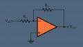
The following diagram conveys the structure of a common destructive charge amplifier.

This is called a floating diffusion amplifier. The floating diffusion is a region of silicon that is not electrically connected to other portions of the circuit. Thus, it’s “floating,” just as we say that an IC pin is floating if it’s left unconnected.
The floating diffusion has some capacitance, and when it receives a packet of charge, its voltage changes according to the typical capacitance equation:
\[V=\frac{Q}{C}\]
Keep in mind that we’re moving electrons into the floating diffusion, so the charge is negative and the voltage decreases. The capacitance of the floating diffusion is small and that’s desirable, because less capacitance leads to more change in voltage relative to charge. One CCD datasheet that I looked at indicated that the voltage presented to the charge amplifier changes by about 20 µV per electron.
Let’s say that a packet of charge has just been deposited into the floating diffusion. No current flows into the gate of M2, and M1 is in the cutoff state, such that the charge can’t be drained away from the floating diffusion. The voltage corresponding to the pixel’s quantity of charge becomes the input signal of M2, which is configured as a source-follower amplifier.
We have many pixels to read out, so after the buffered output voltage is processed by the external circuitry, we need to keep the charge-packet assembly line moving. A reset signal applied to the gate of M1 allows the charge in the floating diffusion to drain away toward the reset-voltage node:

When all the charge from the current pixel has been cleared, we can shift in the next charge packet, and the cycle continues.
The CCD Output Signal
The readout operation performed by a CCD results in an analog output waveform that has a very particular shape. If at some point you need to spend long hours in the lab looking at CCD signals, it’s the sort of waveform that gets burned in your memory and becomes permanently associated with digital imaging. This is the general idea:

The plot doesn’t indicate any actual voltage values, for two reasons: First, the DC offset of the output signal varies from CCD to CCD and can be shifted by external circuitry. Second, the signal is sampled in a differential fashion, meaning that the digital pixel value depends not on an absolute voltage but rather on the difference between the voltage at two separate sampling instants. We’ll talk about this more in the next article.
A CCD output waveform consists of three sections per pixel.
- The first (corresponding to the highest-amplitude portion shown in the diagram) is called the reset glitch. I believe that this occurs because the reset pulse applied to M1 capacitively couples through the FET and causes a spurious transient voltage.
- The second section is called the reset level or the reference level. Both names make sense because during this part of the waveform, the signal is held at the reset voltage, and this reset voltage functions as a sampling reference.
- The third is the data level. This is where we actually see the analog voltage value corresponding to the amount of light received by a given pixel.

Conclusion
We’ve covered charge amplifiers and basic characteristics of the analog waveforms produced by a CCD image sensor. In the next article, we’ll discuss techniques that allow us to extract high-quality digital data from a CCD signal.
Related Content


Robert, This is one of the clearest and easiest to understand descriptions I have seen. Thank you.
I realize from this that my application requires tracking the actual voltage. So instead of a load I need to put the signal through an amplifier and then high sampling rate ADC.
The charge of one electron is 1.6022E-19 Coulomb, so the capacitance in the well with 20 microvolt change is
C = Q/V = 1.6022E-19 (Joules = Volt*Coulomb)/20E-6 Volts = 8.011E-14 Farad or 80.11 femtoFarad
Is that right? If so, then I can substitute any known capacitance for the “floating diffusion”. Does the “floating diffusion” have any other properties besse temperature and interfacial potentials to worry about? There is some electron scattering depending on temperature and that conversion to heat will show up as an effective resistance. The electrons are moving and have magnetic field, so they should have an effective inductance. The electrons have magnetic moment (using any spin techniques) so the the “floating diffusion” should have time dependent response and a characteristic impulse reponse over a wide spectral region. Because it is a permanent number of electrons (somewhat), then it will have variations over seconds, minutes and hours, so that can be put into the “low frequency” part of the “floating diffusion"s response function.
So microvolt level amplifier, and ADC could track both low frequency and video frequency changes.
For low frequencies if I make the capacitance of the “floating diffusion” large it can be tailored to low frequencies.
I will try to read about “floating diffusion”. There are 24,000 entries on Google for “floating diffusion”.
There should be a corresponding “hole” version?
Richard Collins, The Internet Foundation