 Facebook
 Google
 GitHub
 Linkedin
The Why and How of Pipelining in FPGAs
This article explains pipelining and its implications with respect to FPGAs, i.e., latency, throughput, change in operating frequency, and resource utilization.
This article explains pipelining and its implications with respect to FPGAs, i.e., latency, throughput, change in operating frequency, and resource utilization.
Programming an FPGA (field programmable gate array) is a process of customizing its resources to implement a definite logical function. This involves modeling the program instructions using the FPGA’s basic building blocks like configurable logic blocks (CLBs), dedicated multiplexers, and others to meet the requirements of the digital system.
During the design process, one important criterion to be taken into account is the timing issue inherent in the system, as well as any constraints laid down by the user. One design mechanism which can help a designer achieve this objective is pipelining.
What Is Pipelining?
Pipelining is a process which enables parallel execution of program instructions. You can see a visual representation of a pipelined processor architecture below.
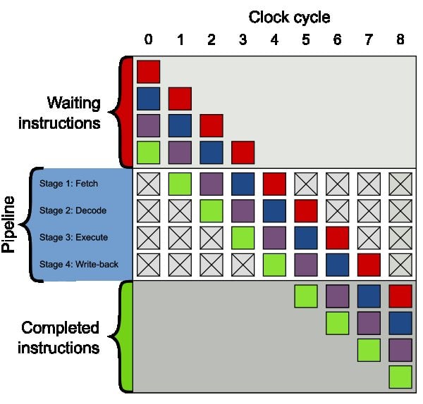
Figure 1. A visual representation of a pipelined processor architecture. Each square corresponds to an instruction. The use of different colors for the squares conveys the fact that the instructions are independent of one another. Image courtesy of Colin M.L. Burnett [CC-BY-SA-3.0].
In FPGAs, this is achieved by arranging multiple data processing blocks in a particular fashion. For this, we first divide our overall logic circuit into several small parts and then separate them using registers (flip-flops).
Let's analyze the mode in which an FPGA design is pipelined by considering an example.
An Example
Let's take a look at a system of three multiplications followed by one addition on four input arrays. Our output yi will therefore be equal to (ai × bi × ci) + di.
Non-Pipelined Design
The first design that comes to mind to create such a system would be multipliers followed by an adder, as shown in Figure 2a.
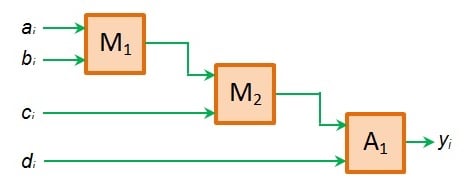
Figure 2a. An example of non-pipelined FPGA design. Image created by Sneha H.L.
Here, we expect the sequence of operations to be the multiplication of ai and bi data by multiplier M1, followed by the multiplication of its product with ci by multiplier M2 and finally the addition of the resultant product with di by adder A1.
Nevertheless, when the system is designed to be synchronous, at the first clock tick, only multiplier M1 can produce valid data at its output (a1 × b1). This is because, at this instant, only M1 has valid data (a1 and b1) at its input pins, unlike M2 and A1.
In the second clock tick, there would be valid data at the input pins of both M1 and M2. However, now we need to ensure that only M2 operates while M1 maintains its output the way it is. This is because, at this instant, if M1 operates, then its output line changes to (a2 × b2) instead of its expected value (a1 × b1) leading to erroneous M2 output (a2 × b2 × c1) and not (a1 × b1 × c1).
When the clock ticks for the third time, there would be valid inputs at all the three components: M1, M2, and A1. Nevertheless, we only want the adder to be operative as we would expect the output to be y1 = (a1 × b1 × c1 + d1). This means the first output of the system will be available after the third clock tick.
Next, as the fourth clock tick arrives, M1 can operate over the next set of data: a2 and b2. But at this instant, M2 and A1 are expected to be idle. This has to be followed by the activation of M2—only M2—at the fifth clock tick and the activation of A1—only A1—at the sixth clock tick. This ensures our next output, y2 = (a2 × b2 × c2 + d2).
When a similar excitation pattern is followed for the components, we can expect the next outputs to occur at clock ticks 9, 12, 15 and so on (Figure 2b).
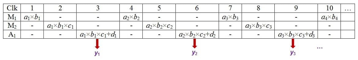
Figure 2b.
Pipelined Design
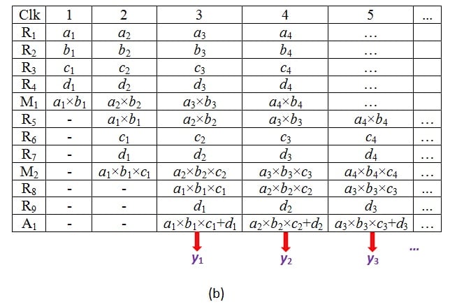
Now, let's suppose that we add registers to this design at the inputs (R1 through R4), between M1 and M2 (R5 and R8, respectively) and along the direct input paths (R6, R7, and R9), as shown by Figure 3a.
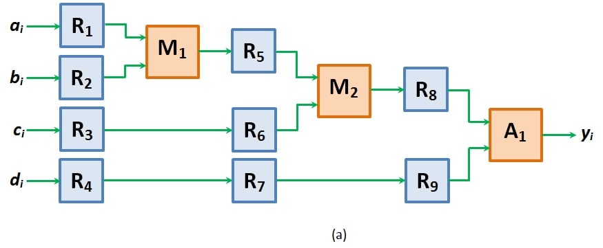
Figure 3a. An example of pipelined FPGA design. Image and table created by Sneha H.L.
Here, at the first clock tick, valid inputs appear only for registers R1 through R4 (a1, b1, c1 and d1, respectively) and for the multiplier M1 (a1 and b1). As a result, only these can produce valid outputs. Moreover, once M1 produces its output, it is passed on to register R5 and stored in it.
At the second clock tick, the values stored in registers R5 and R6 (a1 × b1 and c1) are made to appear as inputs to M2 which enables it to render its output as a1 × b1 × c1, while the output of R4 (d1) is shifted to register R7. Meanwhile, even the second set of data (a2, b2, c2, and d2) enters into the system and appears at the outputs of R1 through R4.
In this case, M1 is allowed to operate on its inputs so as to cause its output line to change from a1 × b1 to a2 × b2, unlike in the case of non-pipelined design. This is because, in this design, any change in the output of M1 does not affect the output of M2. This is because the data required to ensure correct functionality of M2 was already latched in register R5 during the first clock tick (and remains undisturbed even at the second clock tick).
This means insertion of register R5 has made M1 and M2 functionally independent due to which they both can operate on different sets of data at the same time.
Next, when the clock ticks for the third time, the outputs of registers R8 and R9 ((a1 × b1 × c1) and d1) are passed as inputs to adder A1. As a result, we get our first output y1 = ((a1 × b1 × c1) + d1). Nevertheless, at the same clock tick, M1 and M2 will be free to operate on (a3, b3) and (a2, b2, c2), respectively. This is feasible due to the presence of registers R5 isolating block M1 from M2 and R8 isolating multiplier M2 from adder A1.
Thus, at the third clock tick, we would even get (a3 × b3) and (a2 × b2 × c2) from M1 and M2, respectively, in addition to y1.
Now when the fourth clock tick arrives, adder A1 operates on its inputs to yield the second output, y2 = ((a2 × b2 × c2) + d2). In addition, the output of M1 changes from (a3 × b3) to (a4 × b4) while that of M2 changes from (a2 × b2 × c2) to (a3 × b3 × c3).
On following the same mode of operation, we can expect one output data to appear for each clock tick from then on (Figure 3b), unlike in the case of non-pipelined design where we had to wait for three clock cycles to get each single output data (Figure 2b).
Consequences of Pipelining
Latency
In the example shown, pipelined design is shown to produce one output for each clock tick from third clock cycle. This is because each input has to pass through three registers (constituting the pipeline depth) while being processed before it arrives at the output. Similarly, if we have a pipeline of depth n, then the valid outputs appear one per clock cycle only from nth clock tick.
This delay associated with the number of clock cycles lost before the first valid output appears is referred to as latency. The greater the number of pipeline stages, the greater the latency that will be associated with it.
Increase in Operational Clock Frequency
The non-pipelined design shown in Figure 2a is shown to produce one output for every three clock cycles. That is, if we have a clock of period 1 ns, then the input takes 3 ns (3 × 1 ns) to get processed and to appear as output.
This longest data path would then be the critical path, which decides the minimum operating clock frequency of our design. In other words, the frequency of the designed system must be no greater than (1/3 ns) = 333.33 MHz to ensure satisfactory operation.
In the pipelined design, once the pipeline fills, there is one output produced for every clock tick. Thus our operating clock frequency is the same as that of the clock defined (here, it is 1/1ns = 1000 MHz).
These figures clearly indicate that the pipelined design increases the operational frequency considerably when compared to the non-pipelined one.
Increase in Throughput
A pipelined design yields one output per clock cycle (once latency is overcome) irrespective of the number of pipeline stages contained in the design. Hence, by designing a pipelined system, we can increase the throughput of an FPGA.
Greater Utilization of Logic Resources
In pipelining, we use registers to store the results of the individual stages of the design. These components add on to the logic resources used by the design and make it quite huge in terms of hardware.
Conclusion
The act of pipelining a design is quite exhaustive. You need to divide the overall system into individual stages at adequate instants to ensure optimal performance. Nevertheless, the hard work that goes into it is on par with the advantages it renders while the design executes.


really comprehensive and concise!!! I have read many articles about pipeline and been instructed by my supervisor. But this is the first time i have understood it totally.
The best explanation of pipelining concept. thank you for the article