Facebook
 Google
 GitHub
 Linkedin
Comparators
To most people, a comparator is merely an op amp without feedback. With the very large open-loop gain of the op amp, the output abruptly traverses the entire available voltage range when one input passes the level of the other.
This is true for the majority of comparators, but there are also some refinements and variations. Let's examine them, starting with the circuit in Figure 11-1.
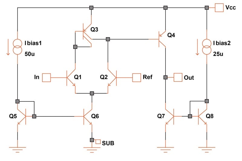
Figure 11-1. A simple but accurate bipolar comparator.
This circuit is indeed of the common variety, being made up of:
- An input differential pair (Q1 and Q2).
- A current-mirror active load (Q3).
- A second stage (Q4).
It gives a voltage gain of about 95 dB.
The second stage is run at half the current compared to the input stage so that it switches when the differential pair is in balance. It uses a separate current mirror (Q7, Q8) for a good reason—Q7 saturates. If we were to run Q7 off Q5, as we do Q6, this saturation would grossly decrease Q6’s collector current.
Current and Voltage Requirements
This comparator, which uses bipolar transistors, requires a small input current. With an operating current of 50 μA (25 μA for each input transistor at balance) and a minimum hFE of 100, that amounts to 0.25 μA. We could, of course, decrease the operating current, but only at the expense of speed and noise.
Also, the reference voltage (in other words, the common-mode voltage) can’t drop below the sum of the VBE of the input transistors and the saturation voltage of Q6. Otherwise, the input stage is simply cut off. The upper end of the common-mode range is about 0.2 V below Vcc, when the input transistors saturate and cut off Q3 and Q4. On the other hand, Vcc can be as low as 1 V.
Simulating a Simple Bipolar Comparator
A simulation for a high-gain circuit like this one is best set up by connecting two voltage sources to the inputs. One is steady DC—say, 1.5 V—while the other one is swept from 1 mV below this value to 1 mV above it. You’ll see the output change drastically very close to the zero difference at the input.
Because Q1, Q2, and both sides of Q3 operate at the same collector-base voltage, there’s very little built-in error. There’s only a small second-order error due to the fact that the collector-base voltage of Q4 is larger. However, don't let this observed accuracy fool you into believing that this is what will happen in production. Move on to a Monte Carlo analysis and you’ll find that the offset voltage of the differential pair moves the switching point by about ± 1 mV, depending on the process and the size of the transistors.
CMOS Comparators
The bipolar design can be directly translated into CMOS, with a logic stage added at the output. Figure 11-2 shows the resulting circuit.

Figure 11-2. CMOS voltage comparator circuit. [click to enlarge]
The gain is now 110 dB. There’s no DC input current, but the previous limitations on the common-mode range still apply.
In a CMOS circuit, you don’t need to fear saturating current mirrors—the current in M8 can be derived from M6. The fact that the drain of M8 can end up very close to the ground has no adverse effect on M7.
A word about the transistor dimensions: the logic stage at the output is designed for a 0.35 μm process. All other channel lengths and widths need to be this large, even for a process capable of smaller sizes.
M1 through M4 require a large area for adequate matching. In fact, the offset can be further reduced by increasing their sizes. The 5 μm channel lengths also reduce dependence on the supply voltage.
Adding Hysteresis to the Comparator
Quite often, hysteresis is required in a comparator. In this context, hysteresis means that the threshold is higher when the input increases and lower when it decreases. For example, say that you have a "low fuel" warning light. You don't want this light to flicker on and off as the fuel sloshes in the tank, so you set the threshold to a low level as the fuel is consumed and to a higher level as the tank is filled.
Figure 11-3 shows a comparator with hysteresis.
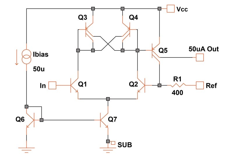
Figure 11-3. Bipolar comparator with hysteresis.
This comparator adds two new features:
- Q3 and Q4 form a flip-flop with precisely controlled gain, giving the circuit a snap action. This replaces the simple current mirror.
- The diode connection of Q4 makes Q5 into a current mirror. Each collector sources one-half of the current.
The current from one of the Q5 collectors is fed into a 400 Ω resistor, causing the reference voltage at the base of Q2 to increase by 10 mV. The resistor value can, of course, be changed to increase or decrease this value. Note that the voltage at Ref must be capable of sinking Q5’s collector current.
As the input voltage decreases from some value above the reference voltage, the current out of the output terminal abruptly increases from zero to about 25 μA. Because of the Early effect, the exact level depends on the output voltage. As Figure 11-4 illustrates, you now have to increase the input voltage to 10 mV above the reference level to turn the output current off.
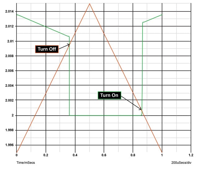
Figure 11-4. Switching input (orange) and output (green) voltages for the bipolar comparator with hysteresis.
A CMOS Version
Figure 11-5 shows the same circuit in CMOS, with the current output (M8) opposed by a current sink of half the level (M13), and a logic stage added.
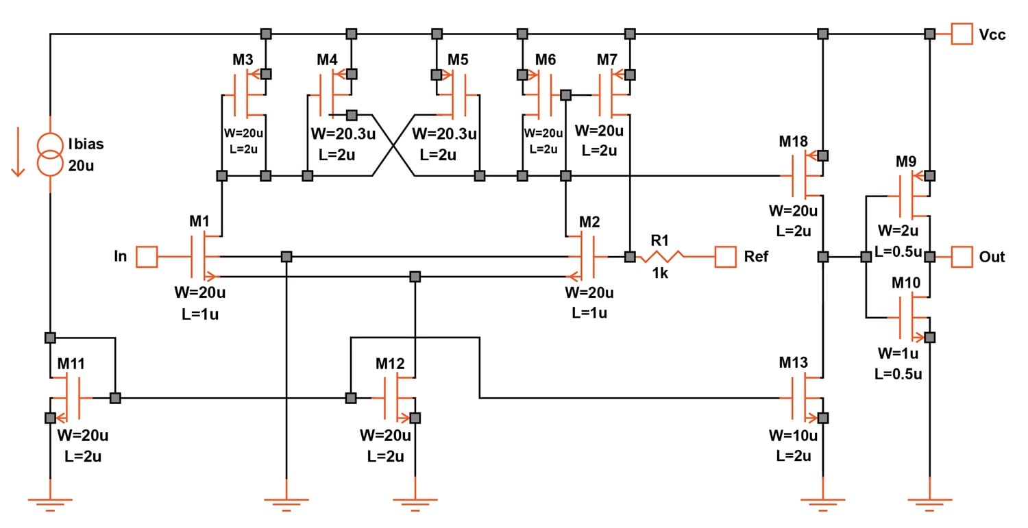
Figure 11-5. CMOS comparator with hysteresis. [click to enlarge]
CMOS has an advantage here—the custom sizing of transistors M3-M6 allows the amount of positive feedback to be set in precise increments.
Note that the operating current (Ibias) has been reduced and the value of R1 increased, resulting again in a hysteresis of 10 mV. Ibias will most likely be derived from a resistor value (and, perhaps, a bandgap reference voltage). R1 will track this resistor value, making the hysteresis remarkably accurate and stable with temperature.
Simulating a Comparator With Hysteresis
A comparator with hysteresis requires some thought before simulating or testing, since the two different thresholds have to be approached in the proper sequence. In a simulation, this can be done with a transient analysis (as demonstrated above in Figure 11-4). We let the input voltage increase until it exceeds the upper threshold, then decrease it until it reaches a level below the lower threshold.
Similarly, in testing, the input is ramped up until switching occurs. It’s then ramped down until the output changes states again.
PNP and P-Channel Comparators
In the examples so far, NPN or N-channel transistors have been used for the input differential pair. Unless you have a split power supply, this is a disadvantage when the input signal and reference are near ground level. By converting the input to PNP or P-channel and with a couple of design refinements, a comparator can be made to work at ground level, even if there is only a single supply. This is illustrated in Figure 11-6.
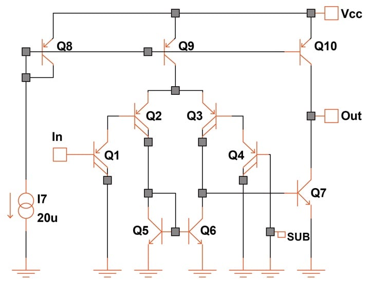
Figure 11-6. A Darlington input allows the inputs to be at ground level.
This circuit uses a Darlington input stage—not to decrease the input current, but to allow the comparator to operate even if the input drops slightly below ground. (Strictly speaking, the input stage is not a pure Darlington connection, since the collectors of Q1 and Q4 go to ground).
With as much as 400 mV below ground at the input, Q1 is still in its active region. At that point, assuming it’s at room temperature, the base of Q2 is about 200 mV above ground. This is sufficient to keep Q5 from being cut off.
This circuit has a definite upper temperature limit of about 100 °C. It is also rather slow because there is no discharge path at the bases of Q2 and Q3. Since the primary object is not a low input current, however, there is no reason why we could not place two additional small current sources (like Q9) at these points.
Comparator With Rail-to-Rail Inputs
Though rarely needed in an ASIC, the ideal comparator has a rail-to-rail input. The CMOS comparator circuits shown above already have rail-to-rail outputs.
This is actually quite easy to achieve. As shown in Figure 11-7, we use two input differential pairs—one N-channel, the other P-channel. We mirror the currents of one and sum the result with the currents of the other.
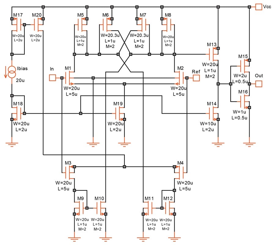
Figure 11-7. CMOS comparator with rail-to-rail inputs. [click to enlarge]
This example uses the same active load as in Figure 11-5. M5–M8 are again sized to provide sufficient positive feedback to give a snap-action. Note that M5–M8 and M9–M12 have a considerably larger width-to-length ratio compared to the corresponding M1–M2 and M3–M4. This allows the input to go slightly beyond Vcc and ground.