Facebook
 Google
 GitHub
 Linkedin
Introduction to Differential Pairs
Open any analog IC, and you’ll find a differential pair. More likely, you’ll find a half dozen. It has great advantages, even when amplifying a "difference" isn’t a goal.
The reasoning is simple: individual integrated components have large variations, but two or more of the same components match very well. If you can take advantage of the matching, you get better performance.
This isn't always true, of course. Noise, for example, can be smaller in a single-transistor stage, and some of the most ingenious designs are remarkably free of the common differential stage.
Still, the differential pair is a wondrous tool. Let’s take a look at it.
The Basic Differential Pair
In a differential pair, a current is divided by two transistors. This is illustrated in Figure 5-1.
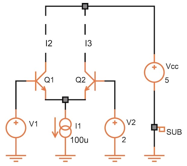
Figure 5-1. In a differential pair, the current I1 is divided by two transistors, Q1 and Q2.
Two transistors—in this case, bipolar—share a common emitter current. If the voltages at their bases are equal and the two transistors match perfectly, I1 is split into two equal parts, I2 and I3, at the collectors.
If we increase V1 relative to V2, Q1 gets more of the current than Q2. If we decrease V1, the opposite is true.
Non-Ideal Behavior of Differential Pairs
There are limitations and errors, however, in the operation of the differential pairs.
Nonlinear Operation
First of all, the current division between the two sides of the differential pair isn’t linear with respect to the input voltages. We’re dealing with two base-emitter diodes here—fundamentally exponential devices. Not counting stray effects, the emitter resistance is:
$$r_e ~=~ \frac {kT}{qI_e}$$
where:
k = the Boltzmann constant (1.38E–23 joules/kelvin)
T = the absolute temperature in kelvin
q = the electron charge (1.6E–19 coulombs)
Ie = the operating current through each emitter
At room temperature (27 °C or 298 K) and with a current of 1 mA, this expression amounts to about 26 Ω:
$$r_e ~=~ \frac {kT}{qI_e} ~=~ \frac{(1.38E-23) \times (298)}{(1.6E-19) \times (1E-3)} ~=~ 25.7 \text{ m}\Omega$$
If Ie drops to 100 μA, re becomes 260 Ω.
Since it’s very much a function of current, re is known as the dynamic emitter resistance. The conversion from base voltage to collector current—the transconductance—is:
$$g_m ~=~ \frac {1}{r_e ~+~R_e}$$
where Re is the ohmic resistance of the emitter—in other words, the resistance between the emitter contact and the emitter-base junction. This is usually a few Ω.
As the current moves from one transistor to the other, both emitter resistances change. We then get some rather nonlinear behavior, as Figure 5-2 shows. Only a small portion of the curve in the middle, when the two currents are equal or nearly equal, could be called linear. In truth, though, that portion isn’t a straight line either.
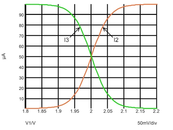
Figure 5-2. The conversion from input voltage to current (the transconductance) is nonlinear.
Temperature Effects
The other variable in the equation is temperature. The emitter resistance is proportional to absolute temperature, so at high temperatures, you get less gain or transconductance. This is illustrated in Figure 5-3.
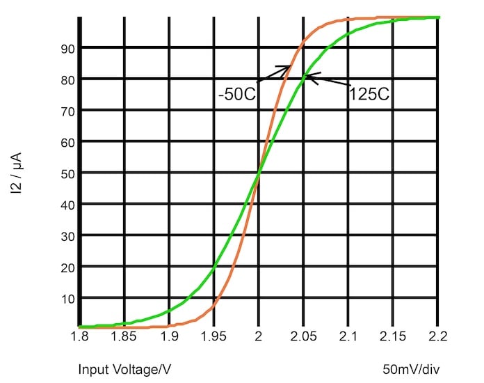
Figure 5-3. The differential pair transconductance is also temperature-dependent.
Errors in Differential Pair Operation
There are also three sources of error to be considered. First of all, a small portion of the emitter current comes from the bases, not the collectors. With a minimum hFE of 100, this makes the sum of the collector current smaller than the emitter current by 1%.
Secondly, transistors only match well if they are operated identically. In this case, that specifically means the collector voltages have to be the same. If one is higher than the other, its transistor will have a higher gain because of the Early effect.
Finally, devices never match perfectly. There will be some differences in both VBE and hFE, and thus some uncertainty in the voltage at which I2 and I3 are equal. This shows up as an offset voltage.
MOS Differential Pairs
A differential pair using MOS transistors (Figure 5-4) behaves almost identically but for entirely different reasons. There’s no dynamic emitter resistance—the gain is determined directly by the transconductance.

Figure 5-4. MOS differential pair.
This transconductance is also nonlinear. As illustrated in Figure 5-5, it increases drastically with increasing gate voltage.
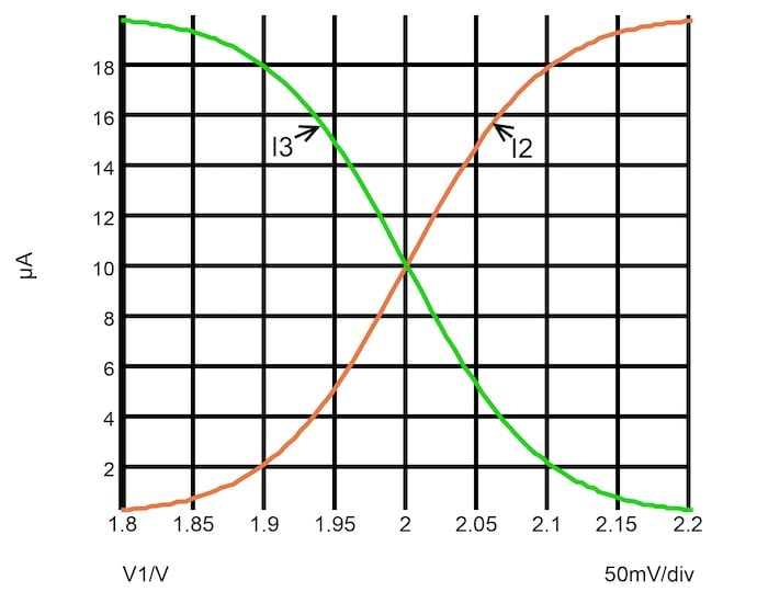
Figure 5-5. A CMOS differential pair is also non-linear.
In the bipolar transistor, size is only of second-order importance. In an MOS transistor, however, transconductance is directly proportional to gate width and decreases with increasing temperature (Figure 5-6).
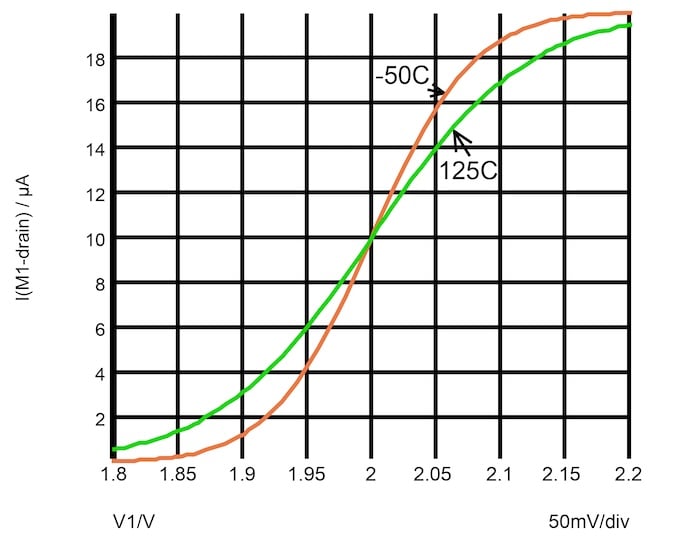
Figure 5-6. The CMOS differential pair transconductance also has a temperature coefficient.
Notably absent in the MOS differential pair error sources is any kind of input current. Here, I2 plus I3 is indeed equal to I1. There is, however, an offset voltage. For equal-sized devices, MOS transistors have a larger offset voltage (mismatch) than bipolar ones. The MOS offset is about 2:1 greater than the bipolar offset, but this depends greatly on the process.
Remember that you can always improve device matching by increasing size (total area). It’s best to do this by using multiple small devices.