Facebook
 Google
 GitHub
 Linkedin
Darlington Pairs for Differential Amplifiers
The base current of a bipolar transistor is a disadvantage. If its operating current is, say, 25 μA and the minimum hFE is 100, the input draws (or supplies, in the case of a PNP transistor) as much as 250 nA. We need something better.
Introducing the Darlington Pair
Sidney Darlington was born in Pittsburgh, Pennsylvania, in 1906 and joined Bell Laboratories in 1929, where he remained until his retirement 42 years later. He was a theorist who also liked to tinker with circuits.
In 1952 silicon transistors made at Bell Labs had low gain (5 to 15). Darlington checked out two of them (only a few were available) and experimented at home over a weekend. He found that by connecting the emitter of one to the base of the other (Figure 5-17), the gain would be the product of the two, 25 to 225, a much more useful range.
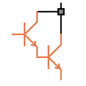
Figure 5-17. The Darlington pair—two bipolar transistors connected together that function as one.
He then suggested a method of fabricating the pair out of a single block of silicon (with a common collector), thus coming very close to the idea of a monolithic integrated circuit. Darlington (and Bell Labs) was issued US patent 2,663,806 for a Semiconductor Signal Translating Device in 1953 (Figure 5-18). Darlington died in 1997 at age 91.
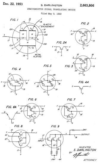
Figure 5-18. Sidney Darlington’s US patent for what became known as the Darlington pair. Image used courtesy of Google Patents
We can decrease the impact of the base current on the differential pair using a Darlington configuration, as shown in Figure 5-19.
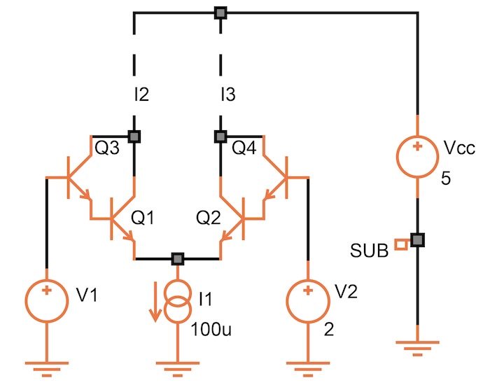
Figure 5-19. NPN Darlington input stage.
Q3 and Q4 carry the base current of the differential pair. At their bases, the input current is reduced by a factor of another hFE. Thus the input current is 5 nA:
$$I_{in} = \frac{I_1}{2(h_{FE})^2} = \frac{100 \text{ }\mu}{2(100)^2} = 5 \text{ nA}$$
There is a price, though:
1. The input voltages need to be higher by a VBE so there is enough headroom for I1.
2. Q3 and Q4 run at very low current; thus, their speed is bound to be rather slow.
3. The leakage currents of Q3 and Q4 run into the bases of Q1 and Q2, showing up multiplied by the hFE of the latter two in I2 and I3. This is a danger at high temperatures (say above 90 °C).
Switching time and leakage current can be reduced with small currents from the emitters of Q3 and Q4 to ground, in effect running the two transistors at a higher operating current. But of course, you can't go too far in that direction: the input current increases again.
As shown in Figure 5-20, if you invert the circuit and use (lateral) PNP transistors at the input, you gain an advantage which is often useful: one input can be at ground.
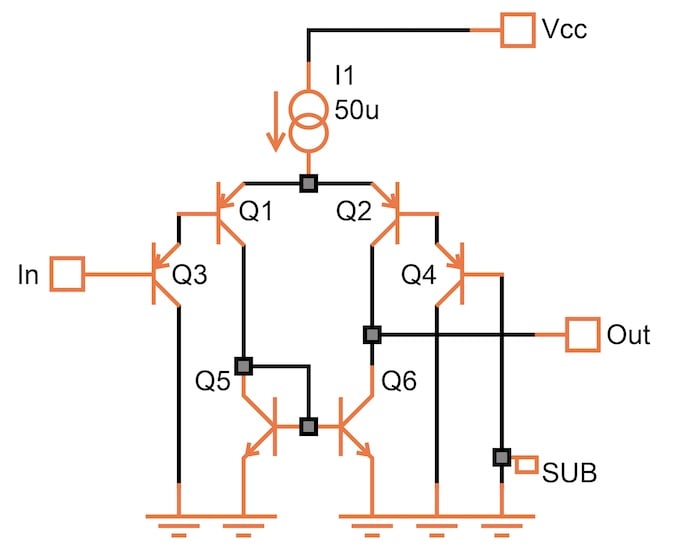
Figure 5-20. A PNP Darlington input stage allows the input to move below ground.
There’s enough headroom for the current mirror (Q5 and Q6) even if the input is 200 or 300 mV below ground. The limit here is one diode drop below ground, at which point the base of Q3 will forward bias against the substrate. The same limitations in speed and upper temperature apply.