 Facebook
 Google
 GitHub
 Linkedin
Differential Pair Amplifiers
Now that we’ve introduced the basic differential pair for both bipolar and MOS circuits, let's get back to bipolar transistors. To complete the differential stage, we can simply use the two collector currents to create voltages across the two resistors, R1 and R2. The result can be seen in Figure 5-7.

Figure 5-7. A complete differential amplifier.
In this example, the voltage at the base of Q2 is held constant at 2 V. This is simply a DC bias voltage large enough to overcome the base-emitter diode voltage. We’re assuming that there is a single 5 V supply.
Vin connects to the base of Q1 and carries the same DC bias level. Vin also has a 50 mV peak AC signal superimposed on the 2 V DC signal so that it moves from 1.95 V to 2.05 V.
Calculating the Differential Gain
The gain of this stage is determined by the ratio of the resistors to the dynamic emitter resistances. Assuming 50 μA of current, we can approximate the dynamic emitter resistance (re) of each transistor by:
$$r_e = \frac{26 \text{ }\Omega \times 1 \text{ mA }}{50 \text{ }\mu \text{A}} = 520 \text{ }\Omega$$
The gain from the inputs to the outputs (G) is given by:
$$G ~=~ \frac {V_{out}}{V_{in}} ~=~ \frac{40 ~\text{ k}\Omega ~+~ 40 ~\text{ k}\Omega}{520~ \text{ }\Omega ~+~ 520~ \text{ }\Omega} ~=~ 77 $$
This gain is measured differentially at both the inputs and outputs. The differential input signal for Figure 5-7 is simply Vin, the 50 mV peak AC signal. The gain to only one output is half of the differential gain.
This circuit doesn’t provide a great deal of gain, and we can’t make that amount any larger by simply increasing the values of R1 and R2. There’s a DC voltage drop of 2 V across the resistors—if we were to double their values, the transistors would saturate.
In reality, the gain is even lower than what we obtain from this simple calculation. The equation doesn’t take into account the ohmic (i.e., access) resistances in the emitters or the fact that a small percentage of the emitter current is lost to the base.
Improving the Linearity with Emitter Resistors
Even with only 50 mV peak input, there is already significant distortion—about 5%. We can improve this by connecting resistors in series with each emitter. The new resistors are labeled as R3 and R4 in Figure 5-8.
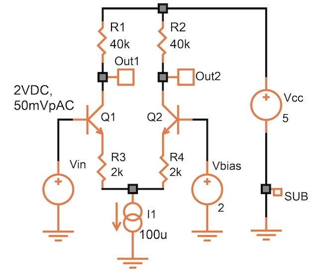
Figure 5-8. Linearized differential amplifier using emitter resistors.
This makes the total emitter resistance more linear, which drops the distortion to less than 0.1% (with a 50 mV peak input). However, the gain suffers badly—it’s less than 16 with a differential output. Single-ended, it’s less than 8.
There is a competing approach. As shown in Figure 5-9, we can replace the single 100 uA emitter current source with two current sources of half the value. In addition, we use a single resistor, R3, of twice the value (4 kΩ) connected between the emitters.
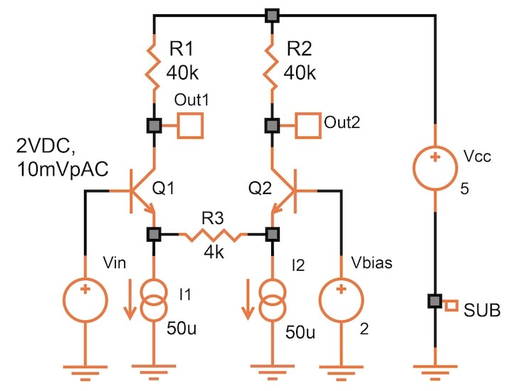
Figure 5-9. An alternative differential amplifier to Figure 5-8 that is identical in performance.
If you take a poll among analog IC designers, about half of them will swear that one is better than the other. In fact, the two circuits are identical in performance.
Active Loads for Improved Differential Amplifier Gain
To get more gain, we need a better scheme for the output. In the vast majority of applications, an amplifier needs only one output. It’s, therefore, no loss if we convert the differential signal to a single-ended one in the very first stage. If we use a current mirror (Figure 5-10), the benefits are immediate.
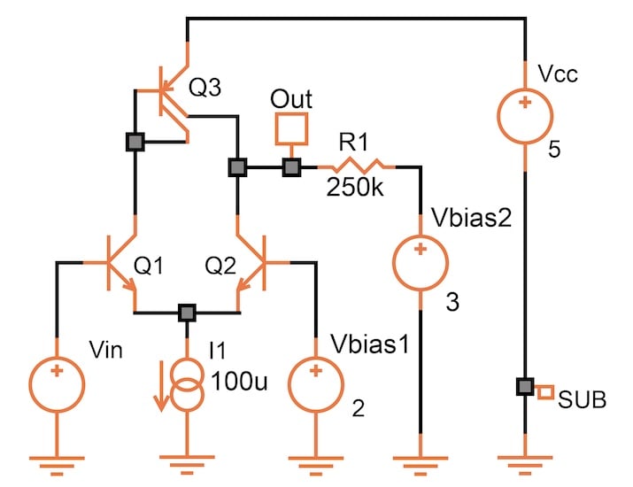
Figure 5-10. Differential amplifier with an active load.
Q3 is called an active load. If one NPN collector current is mirrored by Q3 (here, a split-collector lateral PNP), it opposes the current of the second collector. With no input signal and perfect matching, the two currents are equal. With an input signal, though, one current increases while the other one decreases (hopefully by the same amount) so that we only see their difference at the output. We can, therefore, use a much larger output resistance.
As drawn, the gain of this stage is 278. This large gain produces a large output signal with only 1 mV-peak at the input. As seen in Figure 5–11, this makes the distortion reasonably small.
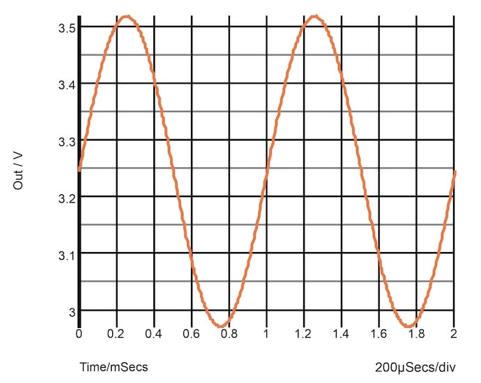
Figure 5-11. Output signal with a 1 mVp sine-wave input.
However, there are two things wrong with the circuit in Figure 5-10. First, if you were to specify a 250 kΩ resistor in an IC, you might be suspected of lunacy—its size would take up more space than all the other components combined.
Second, if you look at the output waveform closely, you’ll notice that there’s a DC current flowing through R1. At the right end, we connect R1 to a 3 V bias point, but at the left end, the center of the sine wave is not 3 V but 3.25 V, meaning we have a built-in offset. There are two reasons for this:
- The two collectors of Q3 are not at the same potential.
- The collector current of Q1 has to supply the base current for Q3.
We need something like R1 to fix the DC potential at the output. The two opposing collectors are current sources/sinks. The smallest difference between the two would cause the output potential to move up so much that Q3 would saturate or down so much that Q2 would saturate.
An Improved Differential Amplifier
Figure 5-12 fixes all of these problems at once by adding a second stage.

Figure 5-12. High-gain, balanced differential amplifier.
In the figure above, Q4 is the same size as Q3 and is operated at the same current. Now, the collector voltages of both Q1/Q2 and Q3 are identical. Moreover, the collector current of Q2 has to supply the same amount of base current (for Q4) as the collector of Q1 does. In other words, with no input signal, the circuit is perfectly balanced—there is no built-in offset.
You need to be careful here, however. The gain of this circuit is no longer fixed by a resistor ratio. Instead, it’s dependent on transistor parameters. If these two stages are made part of an operational amplifier, the feedback will take care of this. Or, if the circuit is used merely as a comparator, the gain is less important than the offset.
If you simulate the circuit as shown, you’ll get the different and rather odd output curve shown in Figure 5-13.

Figure 5-13. Transfer curve for the high-gain, balanced differential amplifier.
Current sources in a simulator are ideal devices—they’ll do anything to supply the exact amount of current, which includes supplying their own voltage (if necessary, thousands of volts).
An actual current sink such as I2 will collapse near ground, but the ideal one keeps right on working down to a very large negative voltage. For this reason, there was an additional device added to the simulation diagram (and not shown in Figure 5-12), a diode from Vin2 to Out which clamps the output swing at the low end.


