Facebook
 Google
 GitHub
 Linkedin
Input Offset Voltage of Differential Amplifiers
The two-stage, high-gain amplifier circuit of Figure 5-14 introduced in our previous section may be perfectly balanced but, as in any circuit, the matching of the devices is still subject to variation.

Figure 5-14. High-gain, balanced differential amplifier.
If we run a Monte Carlo analysis, we meet the real world: the random offset voltage as illustrated in Figure 5-15.

Figure 5-15. Even a perfectly balanced differential amplifier has an offset voltage due to transistor mismatch.
Figure 5-16 shows the same design in CMOS. Note that M3, M4, and M5 are all the same size; thus, balance is achieved with I2 having a magnitude of one-half I1. Here, of course, we are not concerned about the cancellation of base currents, but identical gate voltages are still important.
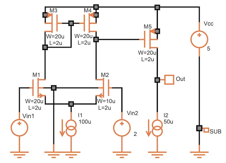
Figure 5-16. Balanced CMOS differential amplifier.
Transistor Matching: Bipolar vs CMOS
The random offset voltage is of greater concern in a CMOS design. MOS transistors match less well than bipolar ones. That has been true since the start of the IC industry. It is not that an MOS transistor is inherently inferior in this respect, but that matching, specifically the offset voltage, is based on different process parameters.
For the bipolar transistor, matching is determined by the depths of diffusions, particularly the base and emitter. The dimension having the greatest influence on offset voltage in an MOS transistor is the gate insulator thickness. While control has steadily increased, the insulator thickness needed to be steadily decreased to get sufficient gain for the ever-smaller devices. The gate insulator thickness has by far the smallest dimension in an IC and thus continues to create fluctuations in threshold voltage larger than a diffusion will cause in VBE.