Facebook
 Google
 GitHub
 Linkedin
Simulating JFET Circuits Using LTspice
The JFET is less prevalent than the metal–oxide–semiconductor field-effect transistor (MOSFET). However, there are many integrated and discrete applications where JFETs are better suited. For example, JFETs can be ideal for audio applications because of their remarkably low noise. When designing circuits based around JFETs, simulation tools such as LTspice can be used to verify the functionality of the circuit.
This chapter provides a basic walkthrough of using LTspice for simulating circuits containing JFETs, and, assuming that the reader has a basic familiarity with LTspice, only key concepts related to JFETs will be discussed.
JFET Equations Overview and the Shockley Equation
First, depending on the gate-source and drain-source voltages (vGS and vDS), JFETs can operate in either the triode or saturation region. As an example, the characteristic curves of an n-channel JFET with IDSS = 8 mA and VP = -4 V are shown in Figure 1.
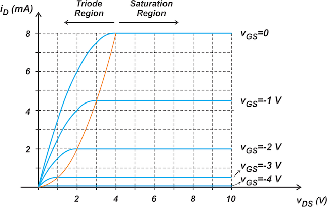
Figure 1. N-channel JFET I-V characteristic curves.
For a given gate-source voltage, when VDS is below the threshold value specified by the orange curve, the JFET is in the triode region. The textbook equation for the drain current of an n-channel JFET in the triode region is shown in Equation 1.
$$i_D = \frac{I_{DSS}}{V_P^2} \Big ( 2(v_{GS}-V_P)-v_{DS} \Big )v_{DS} \quad when \quad \begin{cases} v_{GS} > V_P \\ v_{DS} \leq v_{GS}-V_P \end{cases}$$
Equation 1.
For vDS values above the orange curve, the transistor enters the saturation region. Neglecting the channel length modulation effect, the drain current of the n-channel JFET in the saturation region is given via Equation 2.
$$i_D=I_{DSS} \big ( 1- \frac{v_{GS}}{V_P} \big )^2 \quad when \quad \begin{cases} v_{GS} > V_P \\ v_{DS} \geq v_{GS}-V_P \end{cases}$$
Equation 2.
Equation 2 is known as Shockley’s equation. With the channel length modulation taken into account, the saturation current is modified to become Equation 3.
$$i_D=I_{DSS} \big ( 1- \frac{v_{GS}}{V_P} \big )^2 \big ( 1+ \lambda v_{DS} \big )$$
Equation 3.
In this equation, the channel length modulation term shows how the saturation region current changes with the drain-source voltage, vDS. Keep in mind that, under normal operation, the gate-channel junction of the JFET is reverse-biased, and therefore, for an n-channel JFET, vGS ≤ 0.
JFET SPICE Models
The schematic in Figure 2 shows how SPICE models an n-channel JFET.
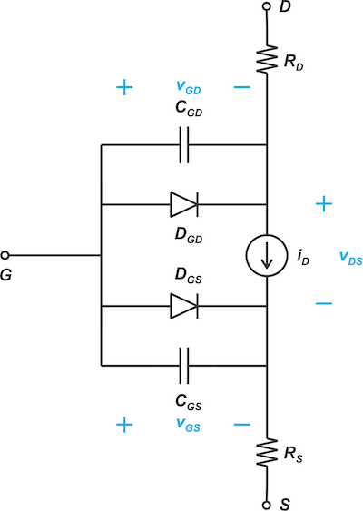
Figure 2. A SPICE schematic representation of an n-channel JFET.
From the basic operation of the JFET, we can expect a current source to appear between the drain and source terminals. Depending on the region of operation, the appropriate equation—for example, Equation 1 or 3—gives the value of the drain current, iD. Resistors RD and RS model the ohmic resistances that appear in series with the drain and source terminals of the physical implementation of the device. Additionally, the gate-channel PN junction is modeled by gate-drain and gate-source diodes, DGD and DGS, while the capacitors in parallel with these diodes—CGD and CGS—model the parasitic capacitances of these junctions. Keep in mind that the capacitance of a reverse-biased PN junction is bias dependent. In the above model, CGD and CGS correspond to the zero-bias condition.
Simulating JFET Circuits Using LTspice
To simulate a circuit containing JFETs, different JFET parameters need to be defined. This can be done by a SPICE .model statement. For example, the LTspice model of the 2N3819, an n-channel JFET from Vishay, is given below:
.model 2N3819 NJF(Beta=1.304m Betatce=-.5 Rd=1 Rs=1 Lambda=2.25m Vto=-3 Vtotc=-2.5m Is=33.57f Isr=322.4f N=1 Nr=2 Xti=3 Alpha=311.7u Vk=243.6 Cgd=1.6p M=.3622 Pb=1 Fc=.5 Cgs=2.414p Kf=9.882E-18 Af=1 mfg=Vishay)
If you look at the parameters inside the parentheses, you’ll recognize some familiar ones, such as CGD, CGS, RD, and RS, that use consistent names with those of the schematic in Figure 2. Also, the parameter Lambda accounts for the channel length modulation effect. However, the two most basic parameters of the JFET—namely IDSS and VP—are not included in the list of parameters. The pinch-off voltage is actually defined as VTO (or Vto) in SPICE models, which is -3 V in the above example (Vto = -3). IDSS is also defined by the Beta parameter according to Equation 4.
$$Beta = \frac{I_{DSS}}{V_P^2}$$
Equation 4.
From here, SPICE uses the following equations to find the drain current iD from vGS and vDS, which can be broken down into Equation 5.
$$i_D=
\begin{cases}
0 & v_{GS} \leq V_T \\
Beta \Big ( 2(v_{GS}-V_T)v_{DS}-v_{DS}^2 \Big ) \times \big ( 1+ \lambda v_{DS} \big ) & v_{GS} > V_T \text{ } and \text{ } v_{DS} \leq v_{GS}-V_T \\
Beta \big ( v_{GS}-V_T \big ) ^2 \times \big ( 1+ \lambda v_{DS} \big ) & v_{GS} > V_T \text{ } and \text{ } v_{DS} \geq v_{GS}-V_T
\end{cases}$$
Equation 5.
In the above equations, SPICE parameters Vto and Lambda are denoted by VT and λ for simplicity. Note that these equations are the same as Equations 1 and 3, except that the triode region equation now includes an additional term to account for the channel length modulation.
Example—Using LTspice to Find the DC Operating Point
In this section, we'll use LTspice to find the DC operating point of the circuit in Figure 3.
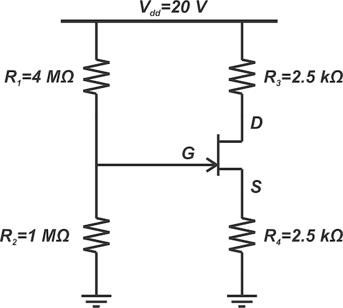
Figure 3. A simple JFET biasing circuit.
In this example, we'll be using the JFET parameters:
- VP = -2 V
- IDSS = 8 mA
- λ = 0.02 V-1
Now that we've established the basics, next is hand calculations! Under normal operating conditions, the gate-channel junction of the JFET is reverse-biased, and the gate current is negligible. Therefore, the gate voltage is determined by the resistive voltage divider formed by R1 and R2, leading to:
$$v_G = \frac{1 M \Omega}{1 M \Omega + 4 M \Omega}\times 20 \text{ }V=4 \text{ }V$$
Having vG, we can express the gate-source voltage as Equation 6
$$v_{GS} = v_{G}-R_4 i_{D}=4- 2.5 i_{D}$$
Equation 6.
Assuming that the transistor is in the saturation region, iD and vGS should also satisfy Equation 2; you can neglect channel length modulation for simplicity. Substituting IDSS = 8 mA and VP = -2 V into this equation produces Equation 7.
$$i_D=8 \big ( 1+ \frac{v_{GS}}{2} \big )^2$$
Equation 7.
The common solutions of Equations 7 and 6 are
$$i_{D}=2 \text{ }mA, \text{ } v_{GS}=-1 \text{ }V$$
and
$$i_{D}=2.88 \text{ }mA, \text{ } v_{GS}=-3.2 \text{ }V$$
Note that only the first solution is valid because, with the second one, vGS is more negative than the pinch-off voltage, and we know that the transistor is in the cut-off region for vGS ≤ VP. The above analysis is based on the assumption that the transistor is in the saturation region. To verify this, we should ensure that vDS ≥ vGS - VP. By applying Kirchhoff’s voltage law to the drain-source brach, we get:
$$v_{DS}=V_{dd}-(R_3 + R_4) \times i_{D}=20-(2.5+2.5)\times 2 =10 \text{ }V$$
This is greater than the minimum vDS for saturation, which is vGS - VP = -1-(-2) = 1 V. Thus, the analysis is valid.
Next, we’ll use LTspice to find the operating point of the above circuit.
Adding a JFET to Your Schematic
The LTspice schematic is shown below in Figure 4.
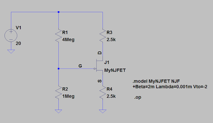
Figure 4. LTspice emulation schematic of the JFET biasing circuit.
To add the n-channel JFET, click on the “Component” button in the LTspice window and type “njf” (Figure 5).
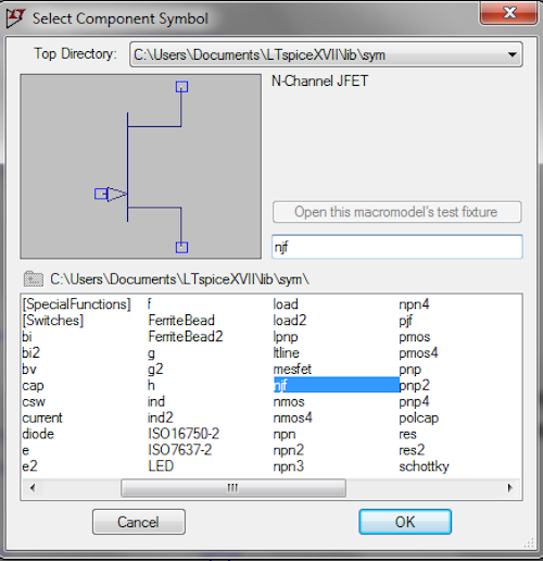
Figure 5. LTspice component selection window.
LTspice includes the model of some common JFET transistors from different vendors. These models are obtained from the device's datasheet specifications. If you're using one of these devices, you can simply select the part number you need. To do this, right-click on the JFET symbol, click “Pick New JFET,” and choose your device from the list (Figure 6).
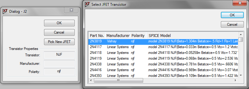
Figure 6. LTspice JFET model selection window.
Adding Third-party Models
If your device is not included in the list or you simply want to experiment with some arbitrary parameter values, you can use a .model statement to describe your JFET to LTspice. To do this, hold down the control key and right-click on the JFET symbol. The new window allows you to edit the component attributes. Here you can enter an arbitrary name for your model in the “Value” field of the symbol. In our example, the model name is “MyNJFET” (Figure 7).
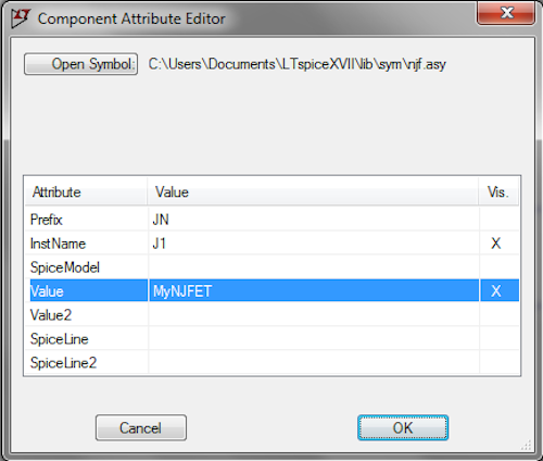
Figure 7. LTspice component attribute editor window.
Lastly, click on the SPICE directive button to add the .model statement. Figure 8 shows the .model statement for our example.
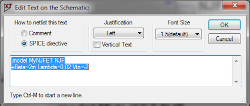
Figure 8. Adding a .model statement to an LTspice schematic.
The parameters Lambda and Vto are straightforward. For Beta, we substitute VP = -2 V and IDSS = 8 mA into Equation 4, leading to Beta = 2 m. As discussed earlier, there are several other device parameters that can be defined in the .model statement. The parameters that are not specified are assigned some default values by SPICE. Here, we can add other components to the schematic and use the .op SPICE derivative to find the operating point of the circuit. On execution, the following results are produced, shown in Figure 9.
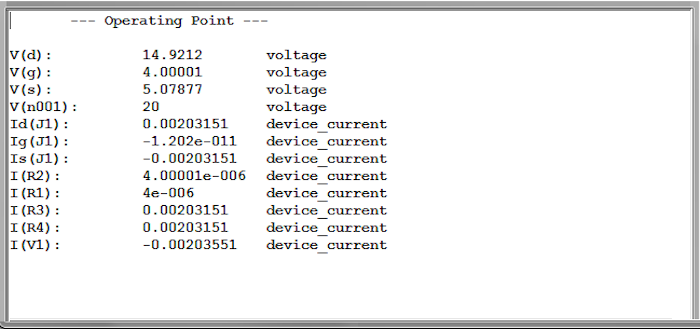
Figure 9. Operating point simulation output for the JFET biasing circuit.
As you can see, the drain current and the gate-source voltage are iD ≅ 2.03 mA and vGS = vG - vS ≅ -1.08 V. These results should agree well with our hand calculations. The discrepancy between the simulation and calculations can partly be attributed to the fact that our hand calculations didn’t account for the channel length modulation effect. In the next sections of this chapter, we’ll explore JFET amplifiers and learn about some other useful features of LTspice.
This textbook page was contributed by Dr. Steve Arar