Facebook
 Google
 GitHub
 Linkedin
JFET Biasing Techniques
In analog design, establishing the right operating point for active components is crucial to achieving the desired performance. In the case of JFETs, appropriate biasing techniques can make the circuit less sensitive to variations in device parameters. In this chapter, we’ll explain different biasing methods for JFET devices using an example.
The JFET Biasing Problem Statement
Consider an n-channel JFET with IDSS = 8 mA and VP = -2 V. The transfer characteristic of the JFET in the saturation region is shown in Figure 1.

Figure 1. N-channel JFET I-V curve in saturation.
With that in mind, let's assume that the goal is to bias the JFET at point Q corresponding to iD = 2 mA and vGS = -1 V. There are a few basic biasing methods that we’ll explore below.
Biasing Method 1—the Constant Voltage Bias
The simplest biasing scheme, known as constant voltage bias, is shown in Figure 2.
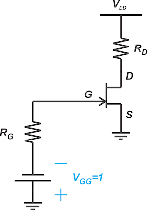
Figure 2. Constant voltage biasing circuit for an n-channel JFET.
Under normal conditions, the gate current of a JFET is essentially zero, and no voltage drops across RG. Thus, the voltage source, VGG, directly appears across the source-gate junction—i.e., vGS = -VGG. By choosing VGG = 1, we can set the bias point to vGS = -1 V. To find the drain current, we can simply substitute the following into Shockley's equation, shown in Equation 1:
- IDSS = 8 mA
- VP = -2 V
- vGS = -1 V
$$i_D=I_{DSS} \big ( 1- \frac{v_{GS}}{V_P} \big )^2$$
Equation 1.
Which produces iD = 2 mA.
In addition, a graphical approach can be employed to determine the DC operating point of the above circuit. To do this, we find the intersection point of the line vGS = -1 with the device characteristic curve (Figure 3).
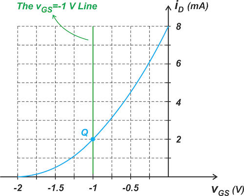
Figure 3. Determining the JFET current for a specific gate-source voltage.
Advantages of the Graphical Approach
The graphical approach can help us develop a more intuitive understanding of the circuit operation. As an example, consider the following circuit (Figure 4), where the input AC signal is applied through the coupling capacitor, C1.
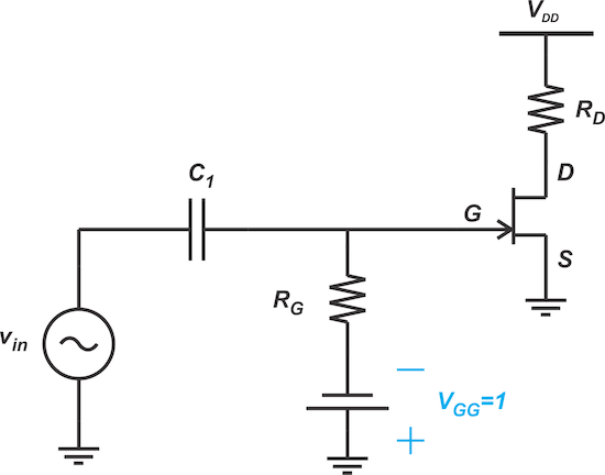
Figure 4. Driving a JFET with an AC-coupled sinusoidal signal.
Let vin be a sinusoidal input with amplitude, A, and assume that the coupling capacitor is sufficiently large so the excursions of vin appear at the gate terminal with no attenuation. In this case, the AC signal adds algebraically to DC bias voltage. Therefore, vGS varies from -1 -A to -1 +A volts. This is illustrated in Figure 5.
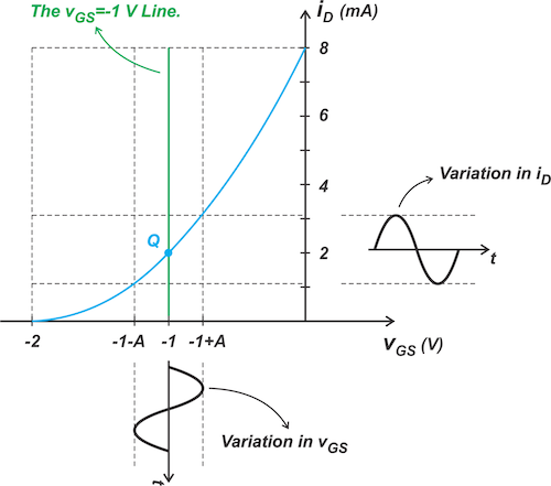
Figure 5. Effect of sinusoidal gate-source voltage variation on the JFET drain current.
By finding the intersection point of the lines corresponding to the maximum and minimum of vGS with the characteristic curve, we can determine the variation in the drain current. In the above example, iD varies from just above 1 mA to slightly higher than 3 mA.
Another advantage of the graphical method is that it helps you visualize how distortion can increase at certain points of the curve. Recall that the slope of the characteristic curve specifies the transconductance of the circuit, which is related to the circuit’s gain. Therefore, a larger curvature in the iD - vGS plot corresponds to a larger distortion. To clarify this, consider the example depicted in Figure 5. Assume that the DC operating point of the circuit is changed to Q1, as depicted below in Figure 6.
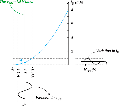
Figure 6. Demonstration of reduced JFET gain as the bias voltage is reduced.
The slope of the curve approaches zero as we get closer and closer to the pinch-off voltage. Therefore, in the above example, the transconductance changes from almost zero to a positive value. Thus, we expect the above circuit to have a larger distortion. Also, note that with the new bias point, the variation in iD is much smaller than in the previous case. This means that the new bias point provides a smaller gain.
Biasing Method 2—the Self-bias Configuration
To avoid the need for two DC supplies, the self-bias configuration shown in Figure 7 can be used.
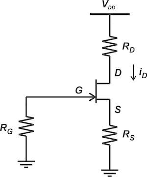
Figure 7. JFET self-biasing circuit schematic.
In this case, the gate is held at zero volts by means of RG; however, the source is at a positive potential because the drain current flows through RS. As a result, a negative vGS is produced without employing a negative voltage supply. Applying Kirchhoff’s voltage law to the input circuit, we get Equation 2.
$$v_{GS}=-R_S i_D$$
Equation 2.
In the case of our example, the bias point is given—iD = 2 mA and vGS = -1 V. Substituting these values into the above equation, we obtain RS = 0.5 kΩ. Usually, RS is given, and we need to find the DC operating point. In this case, Equations 2 and 1 should be solved simultaneously to determine the JFET’s DC operating point. Alternatively, we can use the graphical approach and find the intersection point of the bias line (Equation 2) with JFET's characteristic curve. The graphical solution for RS = 0.5 kΩ is shown in Figure 8.
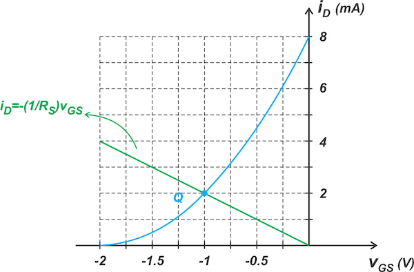
Figure 8. Determining the biasing point for the JFET self-biasing circuit.
Note that the slope of the line is -1/RS. Also, observe that the value of RS is fixed for a given DC operating point. Now consider applying an AC signal to the self-bias configuration (Figure 9).
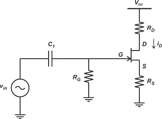
Figure 9. AC coupling a signal to the JFET self-biasing circuit.
Again, assume that the sinusoidal input with amplitude, A, is applied to the input, and the whole signal excursions appear at the gate terminal with no attenuation. Let’s see how the graphical method can be used to find the amplitude of variations in vGS and iD. When the input is at its maximum, the gate voltage is raised from 0 to A volts. Therefore, the bias line is modified to:
$$A=v_{GS}+R_S i_D$$
In the iD - vGS plane, the above equation corresponds to a line with a slope of -1/RS that intercepts the horizontal axis at vGS = A (the orange line in Figure 10).
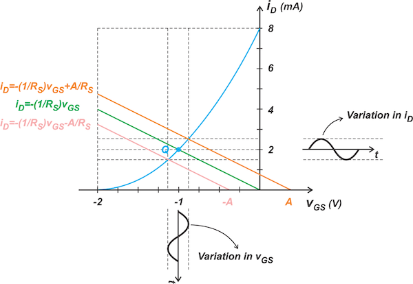
Figure 10. JFET drain current variation as a function of the gate-source voltage variation.
Similarly, when the AC input is at its minimum, the bias line is a line with a slope of -1/RS that intercepts the horizontal axis at vGS = -A (the pink line in the above figure). The intersection points of these lines with the characteristic curve specify the variation in vGS and iD.
Example: Using LTspice to Find JFET Variation in VGS
Use LTspice to find the variation in vGS for the following circuit and compare the results with those of the graphical method. The JFET parameters are:
- VP = -2 V
- IDSS = 8 mA
- λ = 0
Figure 11 shows the schematic for the self-biasing JFET with an AC input.
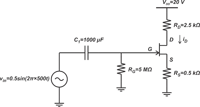
Figure 11. Schematic for the JFET self-biasing circuit with AC input.
Alternatively, the LTspice schematic is shown below in Figure 12.
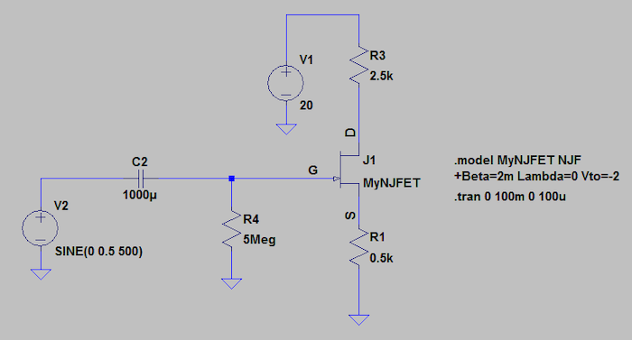
Figure 12. LTspice schematic for the JFET self-biasing circuit with AC input.
Figure 13 provides the simulated vGS waveform.
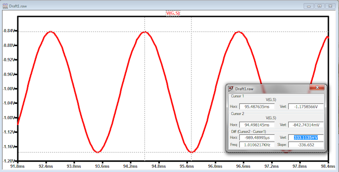
Figure 13. Sinusoidal AC gate-source voltage.
As can be seen, the peak-to-peak variation of vGS is 333 mV. The graphical representation of this problem is shown below in Figure 14.
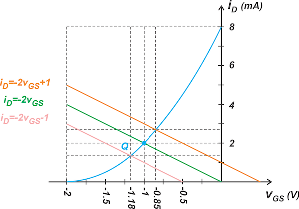
Figure 14. Graphical representation of the change in JFET biasing point for the 333 mV gate-source variation.
From the graphical solution, the vGS variation is found to be -0.85 -(-1.18) = 0.33 V, which is consistent with the simulation results.
Biasing Method 3—the Voltage Divider Biasing
A disadvantage of the self-bias circuit is that the slope of the bias line, which is equal to -1/RS, is fixed for a given DC operating point (Figure 8). In the following chapters of this textbook, we’ll discuss how the ability to choose the slope of the bias line can reduce the sensitivity of the DC operating point to device parameter variations. The voltage divider biasing arrangement, depicted in Figure 15, enables us to choose the slope of the bias line arbitrarily.
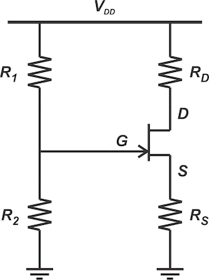
Figure 15. Voltage divider biasing of a JFET.
To find the bias line, note that the gate current is essentially zero, and thus, the gate voltage is specified by the resistive voltage divider made of R1 and R2. Therefore, the gate voltage can be expressed as Equation 3.
$$v_{G}=\frac{R_2}{R_1 + R_2}V_{DD}$$
Equation 3.
Now, applying Kirchhoff’s voltage law to the input circuit produces:
$$\frac{R_2}{R_1 + R_2}V_{DD}=v_{GS}+R_S i_D$$
In the iD - vGS plane, the above equation corresponds to a line with a slope of -1/RS that intercepts the horizontal axis at a vGS value given by Equation 3. Returning to our example, we obtain the graphical representation below in Figure 16.
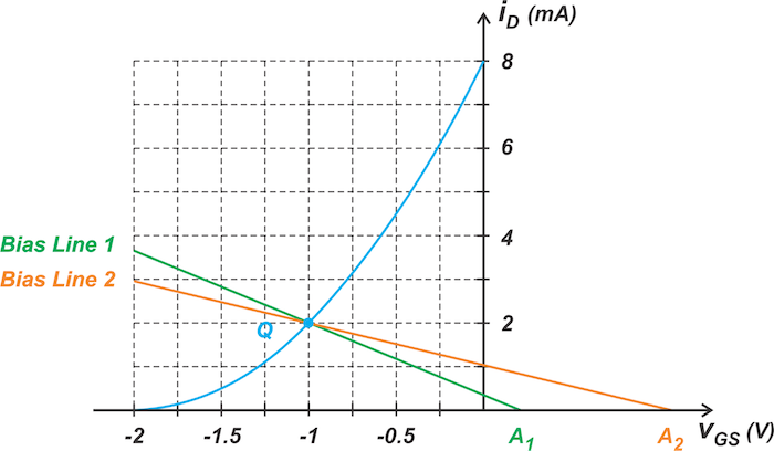
Figure 16. Bias point curves for the JFET circuit with voltage divider biasing.
The above figure shows two possible bias lines that have different slopes and intercept points, A1 and A2. In fact, if we aim to have a particular bias line, we can choose the appropriate RS value to provide the required slope; and then choose parameters, R1 and R2, to adjust the x-axis intercept point. In the next section of this series, we’ll continue this discussion and investigate bias sensitivity to parameter variations.