 Facebook
 Google
 GitHub
 Linkedin
Active-mode Operation (JFET)
JFETs, like bipolar transistors, are able to “throttle” current in a mode between cutoff and saturation called the active mode. To better understand JFET operation, let’s set up a SPICE simulation similar to the one used to explore basic bipolar transistor function:
Spice Simulation of a JFET Operation
jfet simulation vin 0 1 dc 1 j1 2 1 0 mod1 vammeter 3 2 dc 0 v1 3 0 dc .model mod1 njf .dc v1 0 2 0.05 .plot dc i(vammeter) .end
Note that the transistor labeled “Q1” in the schematic is represented in the SPICE netlist as j1. Although all transistor types are commonly referred to as “Q” devices in circuit schematics—just as resistors are referred to by “R” designations and capacitors by “C”—SPICE needs to be told what type of transistor this is by means of a different letter designation: q for bipolar junction transistors and j for junction field-effect transistors.
Here, the controlling signal is a steady voltage of 1 volt, applied with negative towards the JFET gate and positive toward the JFET source, to reverse-bias the PN junction. In the first BJT simulation of chapter 4, a constant-current source of 20 µA was used for the controlling signal, but remember that a JFET is a voltage-controlled device, not a current-controlled device like the bipolar junction transistor.
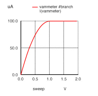
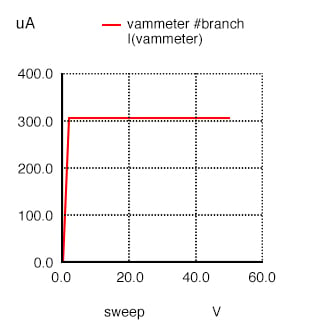
Like the BJT, the JFET tends to regulate the controlled current at a fixed level above a certain power supply voltage, no matter how high that voltage may climb. Of course, this current regulation has limits in real life—no transistor can withstand infinite voltage from a power source—and with enough drain-to-source voltage the transistor will “break down” and drain current will surge. But within normal operating limits the JFET keeps the drain current at a steady level independent of power supply voltage. To verify this, we’ll run another computer simulation, this time sweeping the power supply voltage (V1) all the way to 50 volts:
jfet simulation vin 0 1 dc 1 j1 2 1 0 mod1 vammeter 3 2 dc 0 v1 3 0 dc .model mod1 njf .dc v1 0 50 2 .plot dc i(vammeter) .end
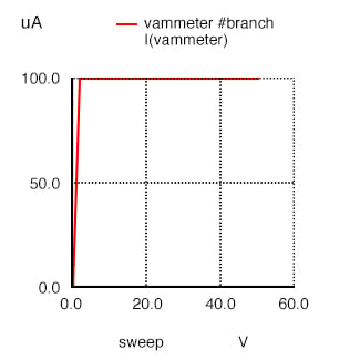
Sure enough, the drain current remains steady at a value of 100 µA (1.000E-04 amps) no matter how high the power supply voltage is adjusted.
Because the input voltage has control over the constriction of the JFET’s channel, it makes sense that changing this voltage should be the only action capable of altering the current regulation point for the JFET, just like changing the base current on a BJT is the only action capable of altering collector current regulation. Let’s decrease the input voltage from 1 volt to 0.5 volts and see what happens:
jfet simulation vin 0 1 dc 0.5 j1 2 1 0 mod1 vammeter 3 2 dc 0 v1 3 0 dc .model mod1 njf .dc v1 0 50 2 .plot dc i(vammeter) .end
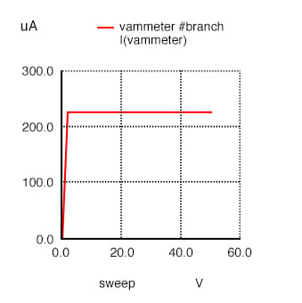
As expected, the drain current is greater now than it was in the previous simulation. With less reverse-bias voltage impressed across the gate-source junction, the depletion region is not as wide as it was before, thus “opening” the channel for charge carriers and increasing the drain current figure.
Please note, however, the actual value of this new current figure: 225 µA (2.250E-04 amps). The last simulation showed a drain current of 100 µA, and that was with a gate-source voltage of 1 volt. Now that we’ve reduced the controlling voltage by a factor of 2 (from 1 volt down to 0.5 volts), the drain current increased, but not by the same 2:1 proportion! Let’s reduce our gate-source voltage once more by another factor of 2 (down to 0.25 volts) and see what happens:
jfet simulation vin 0 1 dc 0.25 j1 2 1 0 mod1 vammeter 3 2 dc 0 v1 3 0 dc .model mod1 njf .dc v1 0 50 2 .plot dc i(vammeter) .end
With the gate-source voltage set to 0.25 volts, one-half what it was before, the drain current is 306.3 µA. Although this is still an increase over the 225 µA from the prior simulation, it isn’t proportional to the change of the controlling voltage.
To obtain a better understanding of what is going on here, we should run a different kind of simulation: one that keeps the power supply voltage constant and instead varies the controlling (voltage) signal. When this kind of simulation was run on a BJT, the result was a straight-line graph, showing how the input current / output current relationship of a BJT is linear. Let’s see what kind of relationship a JFET exhibits:
jfet simulation vin 0 1 dc j1 2 1 0 mod1 vammeter 3 2 dc 0 v1 3 0 dc 25 .model mod1 njf .dc vin 0 2 0.1 .plot dc i(vammeter) .end
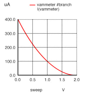
This simulation directly reveals an important characteristic of the junction field-effect transistor: the control effect of gate voltage over drain current is nonlinear. Notice how the drain current does not decrease linearly as the gate-source voltage is increased. With the bipolar junction transistor, collector current was directly proportional to base current: output signal proportionately followed input signal. Not so with the JFET! The controlling signal (gate-source voltage) has less and less effect over the drain current as it approaches cutoff. In this simulation, most of the controlling action (75 percent of drain current decrease—from 400 µA to 100 µA) takes place within the first volt of gate-source voltage (from 0 to 1 volt), while the remaining 25 percent of drain current reduction takes another whole volt worth of input signal. Cutoff occurs at 2 volts input.
Linearity is generally important for a transistor because it allows it to faithfully amplify a waveform without distorting it. If a transistor is nonlinear in its input/output amplification, the shape of the input waveform will become corrupted in some way, leading to the production of harmonics in the output signal. The only time linearity is not important in a transistor circuit is when it's being operated at the extreme limits of cutoff and saturation (off and on, respectively, like a switch).
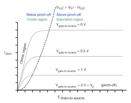
JFET’s Characteristic Curve
A JFET’s characteristic curves display the same current-regulating behavior as for a BJT, and the nonlinearity between gate-to-source voltage and drain current is evident in the disproportionate vertical spacings between the curves:
To better comprehend the current-regulating behavior of the JFET, it might be helpful to draw a model made up of simpler, more common components, just as we did for the BJT:
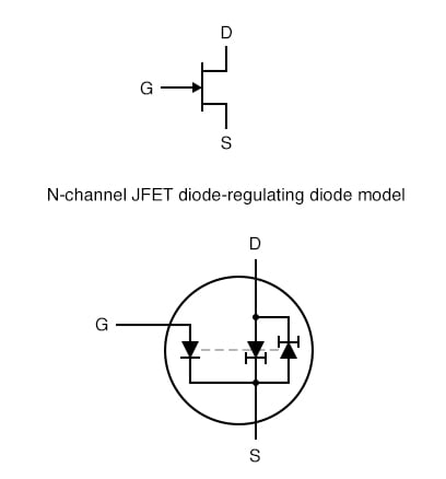
In the case of the JFET, it is the voltage across the reverse-biased gate-source diode which sets the current regulation point for the pair of constant-current diodes. A pair of opposing constant-current diodes is included in the model to facilitate current in either direction between source and drain, a trait made possible by the unipolar nature of the channel. With no PN junctions for the source-drain current to traverse, there is no polarity sensitivity in the controlled current. For this reason, JFETs are often referred to as bilateral devices.
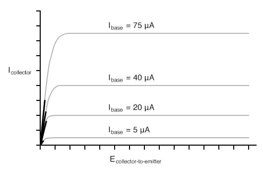
A contrast of the JFET’s characteristic curves against the curves for a bipolar transistor reveals a notable difference: the linear (straight) portion of each curve’s non-horizontal area is surprisingly long compared to the respective portions of a BJT’s characteristic curves:
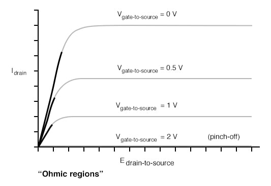
A JFET transistor operated in the triode region tends to act very much like a plain resistor as measured from drain to source. Like all simple resistances, its current/voltage graph is a straight line. For this reason, the triode region (non-horizontal) portion of a JFET’s characteristic curve is sometimes referred to as the ohmic region. In this mode of operation where there isn’t enough drain-to-source voltage to bring drain current up to the regulated point, the drain current is directly proportional to the drain-to-source voltage. In a carefully designed circuit, this phenomenon can be used to an advantage. Operated in this region of the curve, the JFET acts like a voltage-controlled resistance rather than a voltage-controlled current regulator, and the appropriate model for the transistor is different:
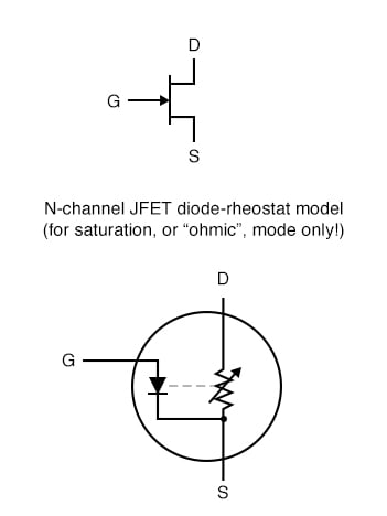
Here and here alone the rheostat (variable resistor) model of a transistor is accurate. It must be remembered, however, that this model of the transistor holds true only for a narrow range of its operation: when it is extremely saturated (far less voltage applied between drain and source than what is needed to achieve full regulated current through the drain). The amount of resistance (measured in ohms) between drain and source in this mode is controlled by how much reverse-bias voltage is applied between gate and source. The less gate-to-source voltage, the less resistance (steeper line on graph).
Because JFETs are voltage-controlled current regulators (at least when they’re allowed to operate in their active), their inherent amplification factor cannot be expressed as a unitless ratio as with BJTs. In other words, there is no β ratio for a JFET. This is true for all voltage-controlled active devices, including other types of field-effect transistors and even electron tubes. There is, however, an expression of controlled (drain) current to controlling (gate-source) voltage, and it is called transconductance. Its unit is Siemens, the same unit for conductance (formerly known as the mho).
Why this choice of units? Because the equation takes on the general form of current (output signal) divided by voltage (input signal).
Transconductance Equation
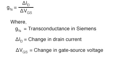
Unfortunately, the transconductance value for any JFET is not a stable quantity: it varies significantly with the amount of gate-to-source control voltage applied to the transistor. As we saw in the SPICE simulations, the drain current does not change proportionally with changes in gate-source voltage. To calculate drain current for any given gate-source voltage, there is another equation that may be used. It is obviously nonlinear upon inspection (note the power of 2), reflecting the nonlinear behavior we’ve already experienced in simulation: 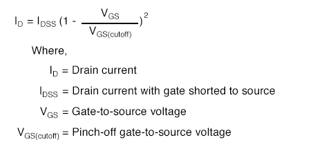
REVIEW:
- In their active modes, JFETs regulate drain current according to the amount of reverse-bias voltage applied between gate and source, much like a BJT regulates collector current according to base current. The mathematical ratio between drain current (output) and gate-to-source voltage (input) is called transconductance, and it is measured in units of Siemens.
- The relationship between gate-source (control) voltage and drain (controlled) current is nonlinear: as gate-source voltage is decreased, drain current increases exponentially. That is to say, the transconductance of a JFET is not constant over its range of operation.
- In their triode region, JFETs regulate drain-to-source resistance according to the amount of reverse-bias voltage applied between gate and source. In other words, they act like voltage-controlled resistances.
RELATED WORKSHEETS:


SPICE models are hard to read. If possible, please rearrange them so each node/component occupies its own line.