
 Facebook
 Google
 GitHub
 Linkedin
Discrete Semiconductor Devices and Circuits
Bipolar Junction Transistor (BJT) theory
28 questions By Tony R. Kuphaldt
-
Question 10 of 28
Match the following bipolar transistor illustrations to their respective schematic symbols:

Reveal answer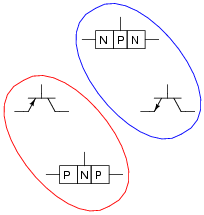
Follow-up question: identify the terminals on each transistor schematic symbol (base, emitter, and collector).
Notes:Be sure to ask your students which of these transistor symbols represents the “NPN” type and which represents the “PNP” type. Although it will be obvious to most from the “sandwich” illustrations showing layers of “P” and “N” type material, this fact may escape the notice of a few students.
It might help to review diode symbols, if some students experience difficulty in matching the designations (PNP versus NPN) with the schematic symbols.
-
Question 11 of 28
If we were to compare the energy diagrams for three pieces of semiconducting material, two “N” type and one “P” type, side-by-side, we would see something like this:
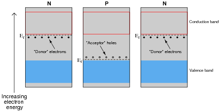
The presence of dopants in the semiconducting materials creates differences in the Fermi energy level (Ef) within each piece.
Draw a new energy diagram showing the equilibrium state of the three pieces after being joined together.
Reveal answer
Notes:If students are familiar with energy band diagrams for PN diode junctions, they should have no great difficulty drawing an energy diagram for an NPN junction.
-
Question 12 of 28
Transistor operation may be explained in terms of three different currents: injection, diffusion, and collection. Describe what each of these currents are, and how they help explain the amplifying nature of a transistor.
Reveal answer“Injection” current consists of those majority charge carriers (either electrons or holes, depending on the transistor type) that are “injected” from the emitter region into the base region of a transistor. “Diffusion” current is the current through the base terminal of the transistor resulting from recombination of electrons and holes in the emitter-base junction. Most of the injection current, however, becomes “collection” current and goes through the collector terminal of the transistor.
Challenge question: explain how the relative doping concentrations of emitter, base, and collector regions is crucial in allowing a transistor to function as an amplifying device. What would happen to the collection current, for example, if the collector were as strongly doped as the emitter?
Notes:As students research and use these terms in their study of bipolar junction transistors, the theory of BJT operation should become more evident. The terms really are well-chosen, accurately representing the motions of charge carriers within the transistor structure.





What surprises me is the following: I did not see any mentioning of the most important BJT parameter: Transconductance gm.
(Instead, you are stating that the beta-value would be a very important parameter - which is NOT the case!).
Like some other low-level electronic books and papers you treat the BJT as a cittent-controlled device - this is simply wrong.
There is not a single proof that the BJT would be a CCCS !
However, there are many theoretical explanations, measurements and observable facts which clearly show that the BJT is - of course - voltage-controlled. Who can deny it ? With which arguments? Ic=beta x Ib is just a formula - a misinterpretation of Ib=Ic/beta.