Facebook
 Google
 GitHub
 Linkedin
Digital Circuits
Design Project: Power Inverter
3 questions By Tony R. Kuphaldt
-
Question 1 of 3
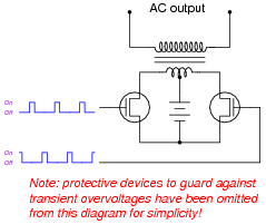
A common topology for DC-AC power converter circuits uses a pair of transistors to switch DC current through the center-tapped winding of a step-up transformer, like this:
In order for this form of circuit to function properly, the transistor “firing” signals must be precisely synchronized to ensure the two are never turned on simultaneously. The following schematic diagram shows a circuit to generate the necessary signals:

Explain how this circuit works, and identify the locations of the frequency control and pulse duty-cycle control potentiometers.
Reveal answerA timing diagram is worth a thousand words:
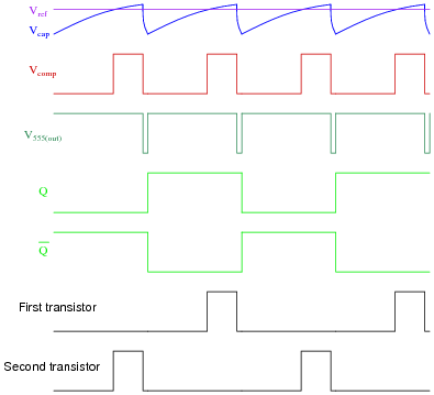
- Vref = DC reference voltage set by duty cycle potentiometer
- Vcap = Voltage measured at top terminal of the 555’s capacitor
- Vcomp = Comparator output voltage
- V555(out) = 555 timer output voltage
- Q = Noninverted output of J-K flip-flop
- [Q] = Inverted output of J-K flip-flop

Follow-up question: which direction would you have to move the frequency potentiometer to increase the output frequency of this circuit? Which direction would you have to move the duty cycle potentiometer to increase that as well?
Challenge question: suppose you were prototyping this circuit without the benefit of an oscilloscope. How could you test the circuit to ensure the final output pulses to the transistors are never simultaneously in the “high” logic state? Assume you had a parts assortment complete with light-emitting diodes and other passive components.
Notes:This question is an exercise in schematic diagram and timing diagram interpretation. By the way, I have built and tested this circuit and I can say it works very well.
-
Question 2 of 3
The zener diodes shown in the schematic are there to absorb transient voltages resulting when the MOSFETs turn off. Explain where these transients originate from, and what might happen if the zener diodes were not there.
Reveal answerEnergy stored in the inductance of the primary winding must go somewhere when the MOSFETs turn off and the magnetic field collapses. Zener diodes provide a safe way to dissipate this stored energy.
Follow-up question: when the inverter circuit runs unloaded (no AC loads connected to the secondary of the transformer), the zener diodes may become warm. Interestingly, these same diodes will cool off when an AC load is connected. Explain why this is.
Notes:Energy storage and transfer are vitally important concepts to grasp for power conversion circuits such as this. The follow-up question was the result of actually testing this inverter circuit and monitoring its performance loaded and unloaded.
-
Question 3 of 3
Examine these check plot images from a PCB drafting program, for a control board based on this inverter circuit design. Both the top and bottom copper layer plots are shown from the perspective of the board’s top side. The six large “pads” around the periphery of the board are actually holes for mounting screws:
Assembly drawing 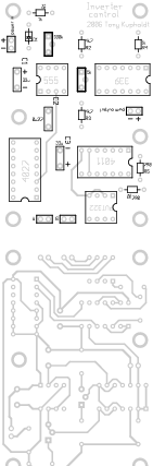
Top copper layer 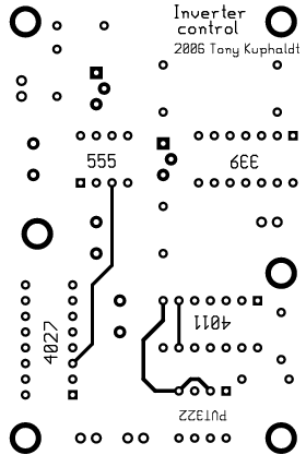
Bottom copper layer 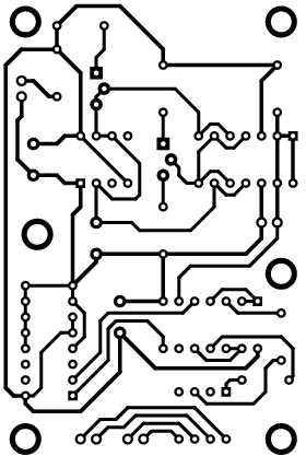
Mark where discrete components (resistors, capacitors, and diodes) go into the PCB, and identify which integrated circuits on the board layout are performing which functions in the schematic. Note: the square pad on each IC marks pin number 1.
Reveal answerI’ll let you do the work on this one. Discuss your answers with your classmates!
Notes:This is an exercise in datasheet research and layout tracing. One potentially confusing aspect of the PCB shown is that I have a diode placed in the circuit for “idiot-proofing” in the event of reverse power supply connections.
In case you were wondering, the reason IC part numbers appear on the “top copper” check plot even though silkscreening is not shown is because I actually wrote the part numbers as part of the copper layer. This was done purely for purposes of economy: my PCB supplier offers a “bare bones” deal with no silkscreening capability, and I still wanted to have IC labels on my boards.